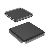
HD6417751RF240V Renesas Electronics America, HD6417751RF240V Datasheet - Page 554

HD6417751RF240V
Manufacturer Part Number
HD6417751RF240V
Description
MPU 1.5/3.3V 0K PB-FREE 256-QFP
Manufacturer
Renesas Electronics America
Series
SuperH® SH7750r
Datasheet
1.D6417751RBP200DV.pdf
(1226 pages)
Specifications of HD6417751RF240V
Core Processor
SH-4
Core Size
32-Bit
Speed
240MHz
Connectivity
EBI/EMI, FIFO, SCI, SmartCard
Peripherals
DMA, POR, WDT
Number Of I /o
39
Program Memory Type
ROMless
Ram Size
48K x 8
Voltage - Supply (vcc/vdd)
1.4 V ~ 1.6 V
Oscillator Type
External
Operating Temperature
-20°C ~ 75°C
Package / Case
256-QFP Exposed Pad, 256-eQFP, 256-HQFP
Lead Free Status / RoHS Status
Lead free / RoHS Compliant
Eeprom Size
-
Program Memory Size
-
Data Converters
-
Available stocks
Company
Part Number
Manufacturer
Quantity
Price
Company:
Part Number:
HD6417751RF240V
Manufacturer:
Renesas Electronics America
Quantity:
10 000
- Current page: 554 of 1226
- Download datasheet (7Mb)
13. Bus State Controller (BSC)
Rev.4.00 Oct. 10, 2008 Page 454 of 1122
REJ09B0370-0400
command, to be completed in the synchronous DRAM. During this cycle, no new command
that accesses the same bank can be issued. In this LSI, the number of Tpc cycles is determined
by the setting of the TPC2 to TPC0 bits of the MCR, and no command that operates on the
synchronous DRAM is issued during these cycles.
Figure 13.39 shows an example of the basic timing of a burst-read. To allow the connection of
a lower-speed DRAM, the cycle's period can be extended by the settings of the bits in WCR2
and MCR. The number of cycles from cycle Tr on which the ACTV command is output to
cycle Tc1 on which the READA command is output can be specified by the RCD1 and RCD0
bits in MCR: the number of cycles is 2, 3, or 4 for the setting value of 1, 2, or 3, respectively.
When two or more cycles are specified, the Trw cycle, which is for the issuing of NOP
commands to the synchronous DRAM, is inserted between the Tr and Tc cycles. The number
of cycles from cycle Tc1 on which the READA command is output until cycle Td1, in which
the first part of the data to be read is received, can be set by the bits A2W2 to A2W0 and
A3W2 to A3W0 of WCR2. These independently select a number of cycles between 1 and 5 for
areas 2 and 3. Note that this number of cycles is equal to the number of CAS latency cycles of
the synchronous DRAM.
Related parts for HD6417751RF240V
Image
Part Number
Description
Manufacturer
Datasheet
Request
R

Part Number:
Description:
KIT STARTER FOR M16C/29
Manufacturer:
Renesas Electronics America
Datasheet:

Part Number:
Description:
KIT STARTER FOR R8C/2D
Manufacturer:
Renesas Electronics America
Datasheet:

Part Number:
Description:
R0K33062P STARTER KIT
Manufacturer:
Renesas Electronics America
Datasheet:

Part Number:
Description:
KIT STARTER FOR R8C/23 E8A
Manufacturer:
Renesas Electronics America
Datasheet:

Part Number:
Description:
KIT STARTER FOR R8C/25
Manufacturer:
Renesas Electronics America
Datasheet:

Part Number:
Description:
KIT STARTER H8S2456 SHARPE DSPLY
Manufacturer:
Renesas Electronics America
Datasheet:

Part Number:
Description:
KIT STARTER FOR R8C38C
Manufacturer:
Renesas Electronics America
Datasheet:

Part Number:
Description:
KIT STARTER FOR R8C35C
Manufacturer:
Renesas Electronics America
Datasheet:

Part Number:
Description:
KIT STARTER FOR R8CL3AC+LCD APPS
Manufacturer:
Renesas Electronics America
Datasheet:

Part Number:
Description:
KIT STARTER FOR RX610
Manufacturer:
Renesas Electronics America
Datasheet:

Part Number:
Description:
KIT STARTER FOR R32C/118
Manufacturer:
Renesas Electronics America
Datasheet:

Part Number:
Description:
KIT DEV RSK-R8C/26-29
Manufacturer:
Renesas Electronics America
Datasheet:

Part Number:
Description:
KIT STARTER FOR SH7124
Manufacturer:
Renesas Electronics America
Datasheet:

Part Number:
Description:
KIT STARTER FOR H8SX/1622
Manufacturer:
Renesas Electronics America
Datasheet:

Part Number:
Description:
KIT DEV FOR SH7203
Manufacturer:
Renesas Electronics America
Datasheet:


