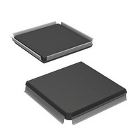
HD6417751RF240V Renesas Electronics America, HD6417751RF240V Datasheet - Page 81

HD6417751RF240V
Manufacturer Part Number
HD6417751RF240V
Description
MPU 1.5/3.3V 0K PB-FREE 256-QFP
Manufacturer
Renesas Electronics America
Series
SuperH® SH7750r
Datasheet
1.D6417751RBP200DV.pdf
(1226 pages)
Specifications of HD6417751RF240V
Core Processor
SH-4
Core Size
32-Bit
Speed
240MHz
Connectivity
EBI/EMI, FIFO, SCI, SmartCard
Peripherals
DMA, POR, WDT
Number Of I /o
39
Program Memory Type
ROMless
Ram Size
48K x 8
Voltage - Supply (vcc/vdd)
1.4 V ~ 1.6 V
Oscillator Type
External
Operating Temperature
-20°C ~ 75°C
Package / Case
256-QFP Exposed Pad, 256-eQFP, 256-HQFP
Lead Free Status / RoHS Status
Lead free / RoHS Compliant
Eeprom Size
-
Program Memory Size
-
Data Converters
-
Available stocks
Company
Part Number
Manufacturer
Quantity
Price
Company:
Part Number:
HD6417751RF240V
Manufacturer:
Renesas Electronics America
Quantity:
10 000
- Current page: 81 of 1226
- Download datasheet (7Mb)
Figure 13.39 Basic Timing of a Burst Read from Synchronous DRAM (Burst Length = 8) ...... 455
Figure 13.40 Basic Timing of a Burst Write to Synchronous DRAM......................................... 456
Figure 13.41 Burst ROM Basic Access Timing .......................................................................... 458
Figure 13.42 Burst ROM Wait Access Timing ........................................................................... 459
Figure 13.43 Burst ROM Wait Access Timing ........................................................................... 460
Figure 13.44 Example of PCMCIA Interface .............................................................................. 464
Figure 13.45 Basic Timing for PCMCIA Memory Card Interface .............................................. 465
Figure 13.46 Wait Timing for PCMCIA Memory Card Interface ............................................... 466
Figure 13.47 PCMCIA Space Allocation .................................................................................... 467
Figure 13.48 Basic Timing for PCMCIA I/O Card Interface ...................................................... 468
Figure 13.49 Wait Timing for PCMCIA I/O Card Interface ....................................................... 469
Figure 13.50 Dynamic Bus Sizing Timing for PCMCIA I/O Card Interface .............................. 470
Figure 13.51 Example of 32-Bit Data Width MPX Connection.................................................. 472
Figure 13.52 MPX Interface Timing 1 (Single Read Cycle, AnW = 0, No External Wait) ........ 473
Figure 13.53 MPX Interface Timing 2 (Single Read, AnW = 0, One External Wait Inserted) ... 474
Figure 13.54 MPX Interface Timing 3 (Single Write Cycle, AnW = 0, No External Wait)........ 475
Figure 13.55 MPX Interface Timing 4 (Single Write, AnW = 1, One External Wait Inserted) . 476
Figure 13.56 MPX Interface Timing 5 (Burst Read Cycle, AnW = 0, No External Wait) .......... 477
Figure 13.57 MPX Interface Timing 6 (Burst Read Cycle, AnW = 0, External Wait Control)... 478
Figure 13.58 MPX Interface Timing 7 (Burst Write Cycle, AnW = 0, No External Wait) ......... 479
Figure 13.59 MPX Interface Timing 8 (Burst Write Cycle, AnW = 1, External Wait Control). 480
Figure 13.60 MPX Interface Timing 9 (Burst Read Cycle, AnW = 0, No External Wait,
Figure 13.61 MPX Interface Timing 10 (Burst Read Cycle, AnW = 0, One External Wait
Figure 13.62 MPX Interface Timing 11 (Burst Write Cycle, AnW = 0, No External Wait,
Figure 13.63 MPX Interface Timing 12 (Burst Write Cycle, AnW = 1, One External Wait
Figure 13.64 Example of 32-Bit Data Width Byte Control SRAM............................................. 485
Figure 13.65 Byte Control SRAM Basic Read Cycle (No Wait) ................................................ 486
Figure 13.66 Byte Control SRAM Basic Read Cycle (One Internal Wait Cycle) ....................... 487
Figure 13.67 Byte Control SRAM Basic Read Cycle (One Internal Wait + One
Figure 13.68 Waits between Access Cycles ................................................................................ 490
Figure 13.69 Arbitration Sequence.............................................................................................. 492
Section 14 Direct Memory Access Controller (DMAC)
Figure 14.1 Block Diagram of DMAC ...................................................................................... 500
Figure 14.2 DMAC Transfer Flowchart .................................................................................... 519
Bus Width: 32 Bits, Transfer Data Size: 64 Bits).................................................. 481
Inserted, Bus Width: 32 Bits, Transfer Data Size: 64 Bits)................................... 482
Bus Width: 32 Bits, Transfer Data Size: 64 Bits).................................................. 483
Inserted, Bus Width: 32 Bits, Transfer Data Size: 64 Bits)................................... 484
External Wait) ........................................................................................................ 488
Rev.4.00 Oct. 10, 2008 Page lxxix of xcviii
REJ09B0370-0400
Related parts for HD6417751RF240V
Image
Part Number
Description
Manufacturer
Datasheet
Request
R

Part Number:
Description:
KIT STARTER FOR M16C/29
Manufacturer:
Renesas Electronics America
Datasheet:

Part Number:
Description:
KIT STARTER FOR R8C/2D
Manufacturer:
Renesas Electronics America
Datasheet:

Part Number:
Description:
R0K33062P STARTER KIT
Manufacturer:
Renesas Electronics America
Datasheet:

Part Number:
Description:
KIT STARTER FOR R8C/23 E8A
Manufacturer:
Renesas Electronics America
Datasheet:

Part Number:
Description:
KIT STARTER FOR R8C/25
Manufacturer:
Renesas Electronics America
Datasheet:

Part Number:
Description:
KIT STARTER H8S2456 SHARPE DSPLY
Manufacturer:
Renesas Electronics America
Datasheet:

Part Number:
Description:
KIT STARTER FOR R8C38C
Manufacturer:
Renesas Electronics America
Datasheet:

Part Number:
Description:
KIT STARTER FOR R8C35C
Manufacturer:
Renesas Electronics America
Datasheet:

Part Number:
Description:
KIT STARTER FOR R8CL3AC+LCD APPS
Manufacturer:
Renesas Electronics America
Datasheet:

Part Number:
Description:
KIT STARTER FOR RX610
Manufacturer:
Renesas Electronics America
Datasheet:

Part Number:
Description:
KIT STARTER FOR R32C/118
Manufacturer:
Renesas Electronics America
Datasheet:

Part Number:
Description:
KIT DEV RSK-R8C/26-29
Manufacturer:
Renesas Electronics America
Datasheet:

Part Number:
Description:
KIT STARTER FOR SH7124
Manufacturer:
Renesas Electronics America
Datasheet:

Part Number:
Description:
KIT STARTER FOR H8SX/1622
Manufacturer:
Renesas Electronics America
Datasheet:

Part Number:
Description:
KIT DEV FOR SH7203
Manufacturer:
Renesas Electronics America
Datasheet:


