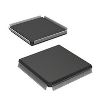
HD6417751RF240V Renesas Electronics America, HD6417751RF240V Datasheet - Page 923

HD6417751RF240V
Manufacturer Part Number
HD6417751RF240V
Description
MPU 1.5/3.3V 0K PB-FREE 256-QFP
Manufacturer
Renesas Electronics America
Series
SuperH® SH7750r
Datasheet
1.D6417751RBP200DV.pdf
(1226 pages)
Specifications of HD6417751RF240V
Core Processor
SH-4
Core Size
32-Bit
Speed
240MHz
Connectivity
EBI/EMI, FIFO, SCI, SmartCard
Peripherals
DMA, POR, WDT
Number Of I /o
39
Program Memory Type
ROMless
Ram Size
48K x 8
Voltage - Supply (vcc/vdd)
1.4 V ~ 1.6 V
Oscillator Type
External
Operating Temperature
-20°C ~ 75°C
Package / Case
256-QFP Exposed Pad, 256-eQFP, 256-HQFP
Lead Free Status / RoHS Status
Lead free / RoHS Compliant
Eeprom Size
-
Program Memory Size
-
Data Converters
-
Available stocks
Company
Part Number
Manufacturer
Quantity
Price
Company:
Part Number:
HD6417751RF240V
Manufacturer:
Renesas Electronics America
Quantity:
10 000
- Current page: 923 of 1226
- Download datasheet (7Mb)
21.1
21.1.1
The high-performance user debug interface (H-UDI) is a serial input/output interface supporting a
subset of the JTAG, IEEE 1149.1, IEEE Standard Test Access Port and Boundary-Scan
Architecture. This LSI H-UDI support boundary-scan, and is used for emulator connection. The
functions of this interface should not be used when using an emulator. Refer to the emulator
manual for the method of connecting the emulator. The H-UDI uses six pins (TCK, TMS, TDI,
TDO, TRST, and ASEBRK/BRKACK). In this LSI, six dedicated emulator pins have been added
(AUDSYNC, AUDCK, and AUDATA3 to AUDATA0). The pin functions and serial transfer
protocol conform to the JTAG specifications.
21.1.2
Figure 21.1 shows a block diagram of the H-UDI. The TAP (test access port) controller and
control registers are reset independently of the chip reset pin by driving the TRST pin low or
setting TMS to 1 and applying TCK for at least five clock cycles. The other circuits are reset and
initialized in an ordinary reset. The H-UDI circuit has six internal registers: SDBPR, SDBSR,
SDIR, SDINT, SDDRH, and SDDRL (these last two together designated SDDR). The SDBPR
register supports the JTAG bypass mode, SDBSR is a shift register forming a JTAG boundary
scan, SDIR is the command register, SDDR is the data register, and SDINT is the H-UDI interrupt
register. SDIR can be accessed directly from the TDI and TDO pins.
Section 21 High-performance User Debug Interface
Overview
Features
Block Diagram
(H-UDI)
21. High-performance User Debug Interface (H-UDI)
Rev.4.00 Oct. 10, 2008 Page 823 of 1122
REJ09B0370-0400
Related parts for HD6417751RF240V
Image
Part Number
Description
Manufacturer
Datasheet
Request
R

Part Number:
Description:
KIT STARTER FOR M16C/29
Manufacturer:
Renesas Electronics America
Datasheet:

Part Number:
Description:
KIT STARTER FOR R8C/2D
Manufacturer:
Renesas Electronics America
Datasheet:

Part Number:
Description:
R0K33062P STARTER KIT
Manufacturer:
Renesas Electronics America
Datasheet:

Part Number:
Description:
KIT STARTER FOR R8C/23 E8A
Manufacturer:
Renesas Electronics America
Datasheet:

Part Number:
Description:
KIT STARTER FOR R8C/25
Manufacturer:
Renesas Electronics America
Datasheet:

Part Number:
Description:
KIT STARTER H8S2456 SHARPE DSPLY
Manufacturer:
Renesas Electronics America
Datasheet:

Part Number:
Description:
KIT STARTER FOR R8C38C
Manufacturer:
Renesas Electronics America
Datasheet:

Part Number:
Description:
KIT STARTER FOR R8C35C
Manufacturer:
Renesas Electronics America
Datasheet:

Part Number:
Description:
KIT STARTER FOR R8CL3AC+LCD APPS
Manufacturer:
Renesas Electronics America
Datasheet:

Part Number:
Description:
KIT STARTER FOR RX610
Manufacturer:
Renesas Electronics America
Datasheet:

Part Number:
Description:
KIT STARTER FOR R32C/118
Manufacturer:
Renesas Electronics America
Datasheet:

Part Number:
Description:
KIT DEV RSK-R8C/26-29
Manufacturer:
Renesas Electronics America
Datasheet:

Part Number:
Description:
KIT STARTER FOR SH7124
Manufacturer:
Renesas Electronics America
Datasheet:

Part Number:
Description:
KIT STARTER FOR H8SX/1622
Manufacturer:
Renesas Electronics America
Datasheet:

Part Number:
Description:
KIT DEV FOR SH7203
Manufacturer:
Renesas Electronics America
Datasheet:


