HD6417751RF240V Renesas Electronics America, HD6417751RF240V Datasheet - Page 23
HD6417751RF240V
Manufacturer Part Number
HD6417751RF240V
Description
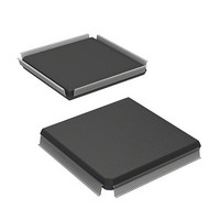
MPU 1.5/3.3V 0K PB-FREE 256-QFP
Manufacturer
Renesas Electronics America
Series
SuperH® SH7750r
Datasheet
1.D6417751RBP200DV.pdf
(1226 pages)
Specifications of HD6417751RF240V
Core Processor
SH-4
Core Size
32-Bit
Speed
240MHz
Connectivity
EBI/EMI, FIFO, SCI, SmartCard
Peripherals
DMA, POR, WDT
Number Of I /o
39
Program Memory Type
ROMless
Ram Size
48K x 8
Voltage - Supply (vcc/vdd)
1.4 V ~ 1.6 V
Oscillator Type
External
Operating Temperature
-20°C ~ 75°C
Package / Case
256-QFP Exposed Pad, 256-eQFP, 256-HQFP
Lead Free Status / RoHS Status
Lead free / RoHS Compliant
Eeprom Size
-
Program Memory Size
-
Data Converters
-
Available stocks
Company
Part Number
Manufacturer
Quantity
Price
Company:

Part Number:
HD6417751RF240V
Manufacturer:
Renesas Electronics America
Quantity:
10 000


Item
12.2.7 Input Capture
Register 2 (TCPR2)
12.4 Interrupts
12.5.4 External Clock
Frequency
13.1.4 Register
Configuration
Table 13.2 BSC
Registers
13.1.6 PCMCIA
Support
Table 13.5 PCMCIA
Support Interfaces
13.2.3 Bus Control
Register 3 (BCR3)
(SH7751R Only)
13.2.7 Wait Control
Register 3 (WCR3)
Page
326
332
333
340
347
359
375
Revision (See Manual for Details)
Title amended
Description amended
There are six TMU interrupt sources, comprising underflow
interrupts and the input capture interrupt (when the input
capture function is used). Underflow interrupts are generated
on channels 0 to 4, and input capture interrupts on channel 2
only.
Description amended
Ensure that the external clock frequency for any channel does
not exceed Pck/8.
Table amended
Name
Bus control register 3*
Table and notes amended
Notes: 1. WP is not supported.
Description amended
BCR3 is initialized to H'0001 by a power-on reset, but is not
initialized by a manual reset or in standby mode.
Description amended of Bits 4n+3
Bits 4n+3⎯Area n (4 or 1) Read-Strobe Negate Timing
(AnRDH) (Setting Only Possible in the SH7751R): When
reading, these bits specify the timing for the negation of read
strobe. These bits should be cleared to 0 when a byte control
SRAM setting is made.
interface.
Note: n = 4 or 1
Pin
57
58
59
Bit 4n + 3: AnRDH
0
1
Corresponding
LSI Pin
—
Output from port
RDY*
2. Input an external wait request with correct polarity.
2
2
Read-Strobe Ne
Read strobe negated after hold wait cycles specified by WCR3.AnH bits
Read strobe negated according to data sampling timing
Abbrevia-
tion
BCR3
Rev.4.00 Oct. 10, 2008 Page xxi of xcviii
R/W
R/W
gate
Timing
Initial
Value
H'0001
Valid only for the SRAM
REJ09B0370-0400
(Initial value)
Related parts for HD6417751RF240V
Image
Part Number
Description
Manufacturer
Datasheet
Request
R

Part Number:
Description:
KIT STARTER FOR M16C/29
Manufacturer:
Renesas Electronics America
Datasheet:

Part Number:
Description:
KIT STARTER FOR R8C/2D
Manufacturer:
Renesas Electronics America
Datasheet:

Part Number:
Description:
R0K33062P STARTER KIT
Manufacturer:
Renesas Electronics America
Datasheet:

Part Number:
Description:
KIT STARTER FOR R8C/23 E8A
Manufacturer:
Renesas Electronics America
Datasheet:

Part Number:
Description:
KIT STARTER FOR R8C/25
Manufacturer:
Renesas Electronics America
Datasheet:

Part Number:
Description:
KIT STARTER H8S2456 SHARPE DSPLY
Manufacturer:
Renesas Electronics America
Datasheet:

Part Number:
Description:
KIT STARTER FOR R8C38C
Manufacturer:
Renesas Electronics America
Datasheet:

Part Number:
Description:
KIT STARTER FOR R8C35C
Manufacturer:
Renesas Electronics America
Datasheet:

Part Number:
Description:
KIT STARTER FOR R8CL3AC+LCD APPS
Manufacturer:
Renesas Electronics America
Datasheet:
Part Number:
Description:
KIT STARTER FOR RX610
Manufacturer:
Renesas Electronics America
Datasheet:

Part Number:
Description:
KIT STARTER FOR R32C/118
Manufacturer:
Renesas Electronics America
Datasheet:

Part Number:
Description:
KIT DEV RSK-R8C/26-29
Manufacturer:
Renesas Electronics America
Datasheet:

Part Number:
Description:
KIT STARTER FOR SH7124
Manufacturer:
Renesas Electronics America
Datasheet:

Part Number:
Description:
KIT STARTER FOR H8SX/1622
Manufacturer:
Renesas Electronics America
Datasheet:

Part Number:
Description:
KIT DEV FOR SH7203
Manufacturer:
Renesas Electronics America
Datasheet: