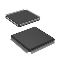
HD6417751RF240V Renesas Electronics America, HD6417751RF240V Datasheet - Page 591

HD6417751RF240V
Manufacturer Part Number
HD6417751RF240V
Description
MPU 1.5/3.3V 0K PB-FREE 256-QFP
Manufacturer
Renesas Electronics America
Series
SuperH® SH7750r
Datasheet
1.D6417751RBP200DV.pdf
(1226 pages)
Specifications of HD6417751RF240V
Core Processor
SH-4
Core Size
32-Bit
Speed
240MHz
Connectivity
EBI/EMI, FIFO, SCI, SmartCard
Peripherals
DMA, POR, WDT
Number Of I /o
39
Program Memory Type
ROMless
Ram Size
48K x 8
Voltage - Supply (vcc/vdd)
1.4 V ~ 1.6 V
Oscillator Type
External
Operating Temperature
-20°C ~ 75°C
Package / Case
256-QFP Exposed Pad, 256-eQFP, 256-HQFP
Lead Free Status / RoHS Status
Lead free / RoHS Compliant
Eeprom Size
-
Program Memory Size
-
Data Converters
-
Available stocks
Company
Part Number
Manufacturer
Quantity
Price
Company:
Part Number:
HD6417751RF240V
Manufacturer:
Renesas Electronics America
Quantity:
10 000
- Current page: 591 of 1226
- Download datasheet (7Mb)
13. Bus State Controller (BSC)
occur simultaneously, priority is given, in high-to-low order, to a bus request from an external
device, a refresh request, the DMAC, and the CPU. See section 13.3.15, Notes on Usage.
To prevent incorrect operation of connected devices when the bus is transferred between master
and slave, all bus control signals are negated before the bus is released. When mastership of the
bus is received, also, bus control signals begin driving the bus from the negated state. Since
signals are driven to the same value by the master and slave exchanging the bus, output buffer
collisions can be avoided.
Bus transfer is executed between bus cycles.
When the bus release request signal (BREQ) is asserted, this LSI releases the bus as soon as the
currently executing bus cycle ends, and outputs the bus use permission signal (BACK). However,
bus release is not performed during multiple bus cycles generated because the data bus width is
smaller than the access size (for example, when performing longword access to 8-bit bus width
memory) or during a 32-byte transfer such as a cache fill or write-back. In addition, bus release is
not performed between read and write cycles during execution of a TAS instruction, or between
read and write cycles when DMAC dual address transfer is executed. When BREQ is negated,
BACK is negated and use of the bus is resumed. See appendix D, Pin Functions, for the pin states
when the bus is released.
When a refresh request is generated, this LSI performs a refresh operation as soon as the currently
executing bus cycle ends. However, refresh operations are deferred during multiple bus cycles
generated because the data bus width is smaller than the access size (for example, when
performing longword access to 8-bit bus width memory) and during a 32-byte transfer such as a
cache fill or write-back, and also between read and write cycles during execution of a TAS
instruction, and between read and write cycles when DMAC dual address transfer is executed.
Refresh operations are also deferred in the bus-released state.
If the synchronous DRAM interface is set to the RAS down mode the PALL command is issued
before a refresh cycle occurs or before the bus is released by bus arbitration.
As the CPU in this LSI is connected to cache memory by a dedicated internal bus, reading from
cache memory can still be carried out when the bus is being used by another bus master inside or
outside this LSI. When writing from the CPU, an external write cycle is generated when write-
through has been set for the cache in this LSI, or when an access is made to a cache-off area.
There is consequently a delay until the bus is returned.
When this LSI wants to take back the bus in response to an internal memory refresh request, it
negates BACK. On receiving the BACK negation, the device that asserted the external bus release
request negates BREQ to release the bus. The bus is thereby returned to this LSI, which then
carries out the necessary processing.
Rev.4.00 Oct. 10, 2008 Page 491 of 1122
REJ09B0370-0400
Related parts for HD6417751RF240V
Image
Part Number
Description
Manufacturer
Datasheet
Request
R

Part Number:
Description:
KIT STARTER FOR M16C/29
Manufacturer:
Renesas Electronics America
Datasheet:

Part Number:
Description:
KIT STARTER FOR R8C/2D
Manufacturer:
Renesas Electronics America
Datasheet:

Part Number:
Description:
R0K33062P STARTER KIT
Manufacturer:
Renesas Electronics America
Datasheet:

Part Number:
Description:
KIT STARTER FOR R8C/23 E8A
Manufacturer:
Renesas Electronics America
Datasheet:

Part Number:
Description:
KIT STARTER FOR R8C/25
Manufacturer:
Renesas Electronics America
Datasheet:

Part Number:
Description:
KIT STARTER H8S2456 SHARPE DSPLY
Manufacturer:
Renesas Electronics America
Datasheet:

Part Number:
Description:
KIT STARTER FOR R8C38C
Manufacturer:
Renesas Electronics America
Datasheet:

Part Number:
Description:
KIT STARTER FOR R8C35C
Manufacturer:
Renesas Electronics America
Datasheet:

Part Number:
Description:
KIT STARTER FOR R8CL3AC+LCD APPS
Manufacturer:
Renesas Electronics America
Datasheet:

Part Number:
Description:
KIT STARTER FOR RX610
Manufacturer:
Renesas Electronics America
Datasheet:

Part Number:
Description:
KIT STARTER FOR R32C/118
Manufacturer:
Renesas Electronics America
Datasheet:

Part Number:
Description:
KIT DEV RSK-R8C/26-29
Manufacturer:
Renesas Electronics America
Datasheet:

Part Number:
Description:
KIT STARTER FOR SH7124
Manufacturer:
Renesas Electronics America
Datasheet:

Part Number:
Description:
KIT STARTER FOR H8SX/1622
Manufacturer:
Renesas Electronics America
Datasheet:

Part Number:
Description:
KIT DEV FOR SH7203
Manufacturer:
Renesas Electronics America
Datasheet:


