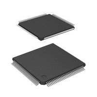
DF2398TE20 Renesas Electronics America, DF2398TE20 Datasheet - Page 262

DF2398TE20
Manufacturer Part Number
DF2398TE20
Description
IC H8S MCU FLASH 256K 120TQFP
Manufacturer
Renesas Electronics America
Series
H8® H8S/2300r
Specifications of DF2398TE20
Core Processor
H8S/2000
Core Size
16-Bit
Speed
20MHz
Connectivity
SCI, SmartCard
Peripherals
DMA, POR, PWM, WDT
Number Of I /o
87
Program Memory Size
256KB (256K x 8)
Program Memory Type
FLASH
Ram Size
8K x 8
Voltage - Supply (vcc/vdd)
4.5 V ~ 5.5 V
Data Converters
A/D 8x10b; D/A 2x8b
Oscillator Type
Internal
Operating Temperature
-20°C ~ 75°C
Package / Case
120-TQFP, 120-VQFP
Lead Free Status / RoHS Status
Contains lead / RoHS non-compliant
Eeprom Size
-
Other names
HD64F2398TE20
HD64F2398TE20
HD64F2398TE20
Available stocks
Company
Part Number
Manufacturer
Quantity
Price
Company:
Part Number:
DF2398TE20V
Manufacturer:
Renesas Electronics America
Quantity:
10 000
- Current page: 262 of 1049
- Download datasheet (5Mb)
If transfer requests are issued simultaneously for more than one channel, or if a transfer request for another channel is
issued during a transfer, when the bus is released the DMAC selects the highest-priority channel from among those issuing
a request according to the priority order shown in table 7-13.
During burst transfer, or when one block is being transferred in block transfer, the channel will not be changed until the
end of the transfer.
Figure 7-35 shows a transfer example in which transfer requests are issued simultaneously for channels 0A, 0B, and 1.
7.5.14
There can be no break between a DMA cycle read and a DMA cycle write. This means that a refresh cycle, external bus
release cycle, or DTC cycle is not generated between the external read and external write in a DMA cycle.
In the case of successive read and write cycles, such as in burst transfer or block transfer, a refresh or external bus released
state may be inserted after a write cycle. Since the DTC has a lower priority than the DMAC, the DTC does not operate
until the DMAC releases the bus.
When DMA cycle reads or writes are accesses to on-chip memory or internal I/O registers, these DMA cycles can be
executed at the same time as refresh cycles or external bus release. However, simultaneous operation may not be possible
when a write buffer is used.
Rev.6.00 Oct.28.2004 page 232 of 1016
REJ09B0138-0600H
Relation between External Bus Requests, Refresh Cycles, the DTC, and the DMAC
Address bus
DMA control
Channel 0A
Channel 0B
Channel 1
HWR
LWR
RD
ø
release
Idle
Bus
Request clear
Read
DMA read
Request
hold
Request
hold
Figure 7-35 Example of Multi-Channel Transfer
Write
Channel 0A
transfer
Selection
DMA write
selection
Non-
Idle
release
Request clear
Bus
Read
DMA read
Request
hold
Write
Channel 0B
transfer
Selection
DMA write
Idle
release
Request clear
Bus
Read
DMA read
Channel 1 transfer
Write
DMA write
Read
DMA
read
Related parts for DF2398TE20
Image
Part Number
Description
Manufacturer
Datasheet
Request
R

Part Number:
Description:
CONN PLUG 12POS DUAL 0.5MM SMD
Manufacturer:
Hirose Electric Co Ltd
Datasheet:

Part Number:
Description:
CONN PLUG 18POS DUAL 0.5MM SMD
Manufacturer:
Hirose Electric Co Ltd
Datasheet:

Part Number:
Description:
CONN PLUG 14POS DUAL 0.5MM SMD
Manufacturer:
Hirose Electric Co Ltd
Datasheet:

Part Number:
Description:
CONN RECEPT 20POS DUAL 0.5MM SMD
Manufacturer:
Hirose Electric Co Ltd
Datasheet:

Part Number:
Description:
CONN PLUG 16POS DUAL 0.5MM SMD
Manufacturer:
Hirose Electric Co Ltd
Datasheet:

Part Number:
Description:
CONN RECEPT 16POS DUAL 0.5MM SMD
Manufacturer:
Hirose Electric Co Ltd
Datasheet:

Part Number:
Description:
CONN PLUG 20POS DUAL 0.5MM SMD
Manufacturer:
Hirose Electric Co Ltd
Datasheet:

Part Number:
Description:
CONN PLUG 30POS DUAL 0.5MM SMD
Manufacturer:
Hirose Electric Co Ltd
Datasheet:

Part Number:
Description:
CONN RECEPT 30POS DUAL 0.5MM SMD
Manufacturer:
Hirose Electric Co Ltd
Datasheet:

Part Number:
Description:
CONN PLUG 40POS DUAL 0.5MM SMD
Manufacturer:
Hirose Electric Co Ltd
Datasheet:

Part Number:
Description:
KIT STARTER FOR M16C/29
Manufacturer:
Renesas Electronics America
Datasheet:

Part Number:
Description:
KIT STARTER FOR R8C/2D
Manufacturer:
Renesas Electronics America
Datasheet:

Part Number:
Description:
R0K33062P STARTER KIT
Manufacturer:
Renesas Electronics America
Datasheet:

Part Number:
Description:
KIT STARTER FOR R8C/23 E8A
Manufacturer:
Renesas Electronics America
Datasheet:

Part Number:
Description:
KIT STARTER FOR R8C/25
Manufacturer:
Renesas Electronics America
Datasheet:


