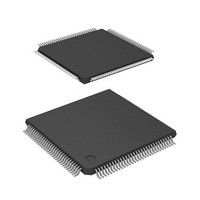
DF2398TE20 Renesas Electronics America, DF2398TE20 Datasheet - Page 521

DF2398TE20
Manufacturer Part Number
DF2398TE20
Description
IC H8S MCU FLASH 256K 120TQFP
Manufacturer
Renesas Electronics America
Series
H8® H8S/2300r
Specifications of DF2398TE20
Core Processor
H8S/2000
Core Size
16-Bit
Speed
20MHz
Connectivity
SCI, SmartCard
Peripherals
DMA, POR, PWM, WDT
Number Of I /o
87
Program Memory Size
256KB (256K x 8)
Program Memory Type
FLASH
Ram Size
8K x 8
Voltage - Supply (vcc/vdd)
4.5 V ~ 5.5 V
Data Converters
A/D 8x10b; D/A 2x8b
Oscillator Type
Internal
Operating Temperature
-20°C ~ 75°C
Package / Case
120-TQFP, 120-VQFP
Lead Free Status / RoHS Status
Contains lead / RoHS non-compliant
Eeprom Size
-
Other names
HD64F2398TE20
HD64F2398TE20
HD64F2398TE20
Available stocks
Company
Part Number
Manufacturer
Quantity
Price
Company:
Part Number:
DF2398TE20V
Manufacturer:
Renesas Electronics America
Quantity:
10 000
- Current page: 521 of 1049
- Download datasheet (5Mb)
Clock: Either an internal clock generated by the on-chip baud rate generator or an external clock input at the SCK pin can
be selected as the SCI’s serial clock, according to the setting of the C/A bit in SMR and the CKE1 and CKE0 bits in SCR.
For details of SCI clock source selection, see table 14-9.
When an external clock is input at the SCK pin, the clock frequency should be 16 times the bit rate used.
When the SCI is operated on an internal clock, the clock can be output from the SCK pin. The frequency of the clock
output in this case is equal to the bit rate, and the phase is such that the rising edge of the clock is in the middle of the
transmit data, as shown in figure 14-3.
Data Transfer Operations:
SCI initialization (asynchronous mode)
Before transmitting and receiving data, you should first clear the TE and RE bits in SCR to 0, then initialize the SCI as
described below.
When the operating mode, transfer format, etc., is changed, the TE and RE bits must be cleared to 0 before making the
change using the following procedure. When the TE bit is cleared to 0, the TDRE flag is set to 1 and TSR is initialized.
Note that clearing the RE bit to 0 does not change the contents of the RDRF, PER, FER, and ORER flags, or the
contents of RDR.
When an external clock is used the clock should not be stopped during operation, including initialization, since
operation is uncertain.
0
Figure 14-3 Relation between Output Clock and Transfer Data Phase
D0
D1
D2
D3
(Asynchronous Mode)
D4
1 frame
D5
D6
D7
0/1
1
Rev.6.00 Oct.28.2004 page 491 of 1016
1
REJ09B0138-0600H
Related parts for DF2398TE20
Image
Part Number
Description
Manufacturer
Datasheet
Request
R

Part Number:
Description:
CONN PLUG 12POS DUAL 0.5MM SMD
Manufacturer:
Hirose Electric Co Ltd
Datasheet:

Part Number:
Description:
CONN PLUG 18POS DUAL 0.5MM SMD
Manufacturer:
Hirose Electric Co Ltd
Datasheet:

Part Number:
Description:
CONN PLUG 14POS DUAL 0.5MM SMD
Manufacturer:
Hirose Electric Co Ltd
Datasheet:

Part Number:
Description:
CONN RECEPT 20POS DUAL 0.5MM SMD
Manufacturer:
Hirose Electric Co Ltd
Datasheet:

Part Number:
Description:
CONN PLUG 16POS DUAL 0.5MM SMD
Manufacturer:
Hirose Electric Co Ltd
Datasheet:

Part Number:
Description:
CONN RECEPT 16POS DUAL 0.5MM SMD
Manufacturer:
Hirose Electric Co Ltd
Datasheet:

Part Number:
Description:
CONN PLUG 20POS DUAL 0.5MM SMD
Manufacturer:
Hirose Electric Co Ltd
Datasheet:

Part Number:
Description:
CONN PLUG 30POS DUAL 0.5MM SMD
Manufacturer:
Hirose Electric Co Ltd
Datasheet:

Part Number:
Description:
CONN RECEPT 30POS DUAL 0.5MM SMD
Manufacturer:
Hirose Electric Co Ltd
Datasheet:

Part Number:
Description:
CONN PLUG 40POS DUAL 0.5MM SMD
Manufacturer:
Hirose Electric Co Ltd
Datasheet:

Part Number:
Description:
KIT STARTER FOR M16C/29
Manufacturer:
Renesas Electronics America
Datasheet:

Part Number:
Description:
KIT STARTER FOR R8C/2D
Manufacturer:
Renesas Electronics America
Datasheet:

Part Number:
Description:
R0K33062P STARTER KIT
Manufacturer:
Renesas Electronics America
Datasheet:

Part Number:
Description:
KIT STARTER FOR R8C/23 E8A
Manufacturer:
Renesas Electronics America
Datasheet:

Part Number:
Description:
KIT STARTER FOR R8C/25
Manufacturer:
Renesas Electronics America
Datasheet:


