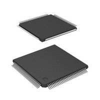
DF2398TE20 Renesas Electronics America, DF2398TE20 Datasheet - Page 629

DF2398TE20
Manufacturer Part Number
DF2398TE20
Description
IC H8S MCU FLASH 256K 120TQFP
Manufacturer
Renesas Electronics America
Series
H8® H8S/2300r
Specifications of DF2398TE20
Core Processor
H8S/2000
Core Size
16-Bit
Speed
20MHz
Connectivity
SCI, SmartCard
Peripherals
DMA, POR, PWM, WDT
Number Of I /o
87
Program Memory Size
256KB (256K x 8)
Program Memory Type
FLASH
Ram Size
8K x 8
Voltage - Supply (vcc/vdd)
4.5 V ~ 5.5 V
Data Converters
A/D 8x10b; D/A 2x8b
Oscillator Type
Internal
Operating Temperature
-20°C ~ 75°C
Package / Case
120-TQFP, 120-VQFP
Lead Free Status / RoHS Status
Contains lead / RoHS non-compliant
Eeprom Size
-
Other names
HD64F2398TE20
HD64F2398TE20
HD64F2398TE20
Available stocks
Company
Part Number
Manufacturer
Quantity
Price
Company:
Part Number:
DF2398TE20V
Manufacturer:
Renesas Electronics America
Quantity:
10 000
- Current page: 629 of 1049
- Download datasheet (5Mb)
19.10.2 Software Protection
Software protection can be implemented by setting the SWE bit in FLMCR1, erase block registers 1 and 2 (EBR1, EBR2),
and the RAMS bit in RAMER. When software protection is in effect, setting the P or E bit in flash memory control
register 1 (FLMCR1) does not cause a transition to program mode or erase mode. (See table 19-17.)
Table 19-17 Software Protection
19.10.3 Error Protection
In error protection, an error is detected when MCU runaway occurs during flash memory programming/erasing, or
operation is not performed in accordance with the program/erase algorithm, and the program/erase operation is aborted.
Aborting the program/erase operation prevents damage to the flash memory due to overprogramming or overerasing.
If the MCU malfunctions during flash memory programming/erasing, the FLER bit is set to 1 in FLMCR2 and the error
protection state is entered. The FLMCR1, FLMCR2, EBR1, and EBR2 settings are retained, but program mode or erase
mode is aborted at the point at which the error occurred. Program mode or erase mode cannot be re-entered by re-setting
the P or E bit. However, PV and EV bit setting is enabled, and a transition can be made to verify mode.
FLER bit setting conditions are as follows:
Error protection is released only by a reset and in hardware standby mode.
Figure 19-21 shows the flash memory state transition diagram.
When flash memory is read during programming/erasing (including a vector read or instruction fetch)
Immediately after exception handling (excluding a reset) during programming/erasing
When a SLEEP instruction (including software standby) is executed during programming/erasing
When the CPU loses the bus during programming/erasing
Item
SWE bit protection
Block specification
protection
Emulation protection
Description
Clearing the SWE bit to 0 in FLMCR1 sets
the program/erase-protected state for all
blocks.
(Execute in on-chip RAM or external
memory.)
Erase protection can be set for individual
blocks by settings in erase block registers
1 and 2 (EBR1, EBR2).
Setting EBR1 and EBR2 to H'00 places all
blocks in the erase-protected state.
Setting the RAMS bit to 1 in the RAM
emulation register (RAMER) places all
blocks in the program/erase-protected
state.
Rev.6.00 Oct.28.2004 page 599 of 1016
Program
Yes
—
Yes
Functions
Erase
Yes
Yes
Yes
REJ09B0138-0600H
Related parts for DF2398TE20
Image
Part Number
Description
Manufacturer
Datasheet
Request
R

Part Number:
Description:
CONN PLUG 12POS DUAL 0.5MM SMD
Manufacturer:
Hirose Electric Co Ltd
Datasheet:

Part Number:
Description:
CONN PLUG 18POS DUAL 0.5MM SMD
Manufacturer:
Hirose Electric Co Ltd
Datasheet:

Part Number:
Description:
CONN PLUG 14POS DUAL 0.5MM SMD
Manufacturer:
Hirose Electric Co Ltd
Datasheet:

Part Number:
Description:
CONN RECEPT 20POS DUAL 0.5MM SMD
Manufacturer:
Hirose Electric Co Ltd
Datasheet:

Part Number:
Description:
CONN PLUG 16POS DUAL 0.5MM SMD
Manufacturer:
Hirose Electric Co Ltd
Datasheet:

Part Number:
Description:
CONN RECEPT 16POS DUAL 0.5MM SMD
Manufacturer:
Hirose Electric Co Ltd
Datasheet:

Part Number:
Description:
CONN PLUG 20POS DUAL 0.5MM SMD
Manufacturer:
Hirose Electric Co Ltd
Datasheet:

Part Number:
Description:
CONN PLUG 30POS DUAL 0.5MM SMD
Manufacturer:
Hirose Electric Co Ltd
Datasheet:

Part Number:
Description:
CONN RECEPT 30POS DUAL 0.5MM SMD
Manufacturer:
Hirose Electric Co Ltd
Datasheet:

Part Number:
Description:
CONN PLUG 40POS DUAL 0.5MM SMD
Manufacturer:
Hirose Electric Co Ltd
Datasheet:

Part Number:
Description:
KIT STARTER FOR M16C/29
Manufacturer:
Renesas Electronics America
Datasheet:

Part Number:
Description:
KIT STARTER FOR R8C/2D
Manufacturer:
Renesas Electronics America
Datasheet:

Part Number:
Description:
R0K33062P STARTER KIT
Manufacturer:
Renesas Electronics America
Datasheet:

Part Number:
Description:
KIT STARTER FOR R8C/23 E8A
Manufacturer:
Renesas Electronics America
Datasheet:

Part Number:
Description:
KIT STARTER FOR R8C/25
Manufacturer:
Renesas Electronics America
Datasheet:


