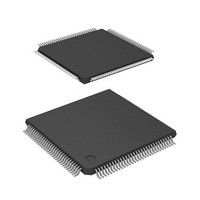
DF2398TE20 Renesas Electronics America, DF2398TE20 Datasheet - Page 572

DF2398TE20
Manufacturer Part Number
DF2398TE20
Description
IC H8S MCU FLASH 256K 120TQFP
Manufacturer
Renesas Electronics America
Series
H8® H8S/2300r
Specifications of DF2398TE20
Core Processor
H8S/2000
Core Size
16-Bit
Speed
20MHz
Connectivity
SCI, SmartCard
Peripherals
DMA, POR, PWM, WDT
Number Of I /o
87
Program Memory Size
256KB (256K x 8)
Program Memory Type
FLASH
Ram Size
8K x 8
Voltage - Supply (vcc/vdd)
4.5 V ~ 5.5 V
Data Converters
A/D 8x10b; D/A 2x8b
Oscillator Type
Internal
Operating Temperature
-20°C ~ 75°C
Package / Case
120-TQFP, 120-VQFP
Lead Free Status / RoHS Status
Contains lead / RoHS non-compliant
Eeprom Size
-
Other names
HD64F2398TE20
HD64F2398TE20
HD64F2398TE20
Available stocks
Company
Part Number
Manufacturer
Quantity
Price
Company:
Part Number:
DF2398TE20V
Manufacturer:
Renesas Electronics America
Quantity:
10 000
- Current page: 572 of 1049
- Download datasheet (5Mb)
16.2
16.2.1
There are four 16-bit read-only ADDR registers, ADDRA to ADDRD, used to store the results of A/D conversion.
The 10-bit data resulting from A/D conversion is transferred to the ADDR register for the selected channel and stored
there. The upper 8 bits of the converted data are transferred to the upper byte (bits 15 to 8) of ADDR, and the lower 2 bits
are transferred to the lower byte (bits 7 and 6) and stored. Bits 5 to 0 are always read as 0.
The correspondence between the analog input channels and ADDR registers is shown in table 16-3.
ADDR can always be read by the CPU. The upper byte can be read directly, but for the lower byte, data transfer is
performed via a temporary register (TEMP). For details, see section 16.3, Interface to Bus Master.
The ADDR registers are initialized to H'0000 by a reset, and in standby mode or module stop mode.
Table 16-3 Analog Input Channels and Corresponding ADDR Registers
16.2.2
Note: * Only 0 can be written to bit 7, to clear this flag.
ADCSR is an 8-bit readable/writable register that controls A/D conversion operations and shows the status of the
operation.
ADCSR is initialized to H'00 by a reset, and in hardware standby mode or module stop mode.
Rev.6.00 Oct.28.2004 page 542 of 1016
REJ09B0138-0600H
Bit
Initial value :
R/W
Bit
Initial value :
R/W
Register Descriptions
A/D Data Registers A to D (ADDRA to ADDRD)
A/D Control/Status Register (ADCSR)
Group 0
AN0
AN1
AN2
AN3
:
:
:
:
AD9 AD8 AD7 AD6 AD5 AD4 AD3 AD2 AD1 AD0 —
15
R
R/(W)*
0
ADF
7
0
14
Analog Input Channel
R
0
13
R
0
ADIE
R/W
6
0
12
R
0
Group 1
AN4
AN5
AN6
AN7
11
R
0
ADST
R/W
5
0
10
R
0
R
9
0
SCAN
R/W
4
0
R
8
0
A/D Data Register
ADDRA
ADDRB
ADDRC
ADDRD
R
7
0
CKS
R/W
3
0
R
6
0
R
5
0
CH2
R/W
2
0
—
R
4
0
—
R
3
0
CH1
R/W
1
0
—
R
2
0
—
R
1
0
CH0
R/W
0
0
—
R
0
0
Related parts for DF2398TE20
Image
Part Number
Description
Manufacturer
Datasheet
Request
R

Part Number:
Description:
CONN PLUG 12POS DUAL 0.5MM SMD
Manufacturer:
Hirose Electric Co Ltd
Datasheet:

Part Number:
Description:
CONN PLUG 18POS DUAL 0.5MM SMD
Manufacturer:
Hirose Electric Co Ltd
Datasheet:

Part Number:
Description:
CONN PLUG 14POS DUAL 0.5MM SMD
Manufacturer:
Hirose Electric Co Ltd
Datasheet:

Part Number:
Description:
CONN RECEPT 20POS DUAL 0.5MM SMD
Manufacturer:
Hirose Electric Co Ltd
Datasheet:

Part Number:
Description:
CONN PLUG 16POS DUAL 0.5MM SMD
Manufacturer:
Hirose Electric Co Ltd
Datasheet:

Part Number:
Description:
CONN RECEPT 16POS DUAL 0.5MM SMD
Manufacturer:
Hirose Electric Co Ltd
Datasheet:

Part Number:
Description:
CONN PLUG 20POS DUAL 0.5MM SMD
Manufacturer:
Hirose Electric Co Ltd
Datasheet:

Part Number:
Description:
CONN PLUG 30POS DUAL 0.5MM SMD
Manufacturer:
Hirose Electric Co Ltd
Datasheet:

Part Number:
Description:
CONN RECEPT 30POS DUAL 0.5MM SMD
Manufacturer:
Hirose Electric Co Ltd
Datasheet:

Part Number:
Description:
CONN PLUG 40POS DUAL 0.5MM SMD
Manufacturer:
Hirose Electric Co Ltd
Datasheet:

Part Number:
Description:
KIT STARTER FOR M16C/29
Manufacturer:
Renesas Electronics America
Datasheet:

Part Number:
Description:
KIT STARTER FOR R8C/2D
Manufacturer:
Renesas Electronics America
Datasheet:

Part Number:
Description:
R0K33062P STARTER KIT
Manufacturer:
Renesas Electronics America
Datasheet:

Part Number:
Description:
KIT STARTER FOR R8C/23 E8A
Manufacturer:
Renesas Electronics America
Datasheet:

Part Number:
Description:
KIT STARTER FOR R8C/25
Manufacturer:
Renesas Electronics America
Datasheet:


