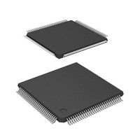
DF2398TE20 Renesas Electronics America, DF2398TE20 Datasheet - Page 577

DF2398TE20
Manufacturer Part Number
DF2398TE20
Description
IC H8S MCU FLASH 256K 120TQFP
Manufacturer
Renesas Electronics America
Series
H8® H8S/2300r
Specifications of DF2398TE20
Core Processor
H8S/2000
Core Size
16-Bit
Speed
20MHz
Connectivity
SCI, SmartCard
Peripherals
DMA, POR, PWM, WDT
Number Of I /o
87
Program Memory Size
256KB (256K x 8)
Program Memory Type
FLASH
Ram Size
8K x 8
Voltage - Supply (vcc/vdd)
4.5 V ~ 5.5 V
Data Converters
A/D 8x10b; D/A 2x8b
Oscillator Type
Internal
Operating Temperature
-20°C ~ 75°C
Package / Case
120-TQFP, 120-VQFP
Lead Free Status / RoHS Status
Contains lead / RoHS non-compliant
Eeprom Size
-
Other names
HD64F2398TE20
HD64F2398TE20
HD64F2398TE20
Available stocks
Company
Part Number
Manufacturer
Quantity
Price
Company:
Part Number:
DF2398TE20V
Manufacturer:
Renesas Electronics America
Quantity:
10 000
- Current page: 577 of 1049
- Download datasheet (5Mb)
On completion of conversion, the ADF flag is set to 1. If the ADIE bit is set to 1 at this time, an ADI interrupt request is
generated. The ADF flag is cleared by writing 0 after reading ADCSR.
When the operating mode or analog input channel must be changed during analog conversion, to prevent incorrect
operation, first clear the ADST bit to 0 in ADCSR to halt A/D conversion. After making the necessary changes, set the
ADST bit to 1 to start A/D conversion again. The ADST bit can be set at the same time as the operating mode or input
channel is changed.
Typical operations when channel 1 (AN1) is selected in single mode are described next. Figure 16-3 shows a timing
diagram for this example.
[1] Single mode is selected (SCAN = 0), input channel AN1 is selected (CH2 = 0, CH1 = 0, CH0 = 1), the A/D interrupt is
[2] When A/D conversion is completed, the result is transferred to ADDRB. At the same time the ADF flag is set to 1, the
[3] Since ADF = 1 and ADIE = 1, an ADI interrupt is requested.
[4] The A/D interrupt handling routine starts.
[5] The routine reads ADCSR, then writes 0 to the ADF flag.
[6] The routine reads and processes the connection result (ADDRB).
[7] Execution of the A/D interrupt handling routine ends. After that, if the ADST bit is set to 1, A/D conversion starts
enabled (ADIE = 1), and A/D conversion is started (ADST = 1).
ADST bit is cleared to 0, and the A/D converter becomes idle.
again and steps [2] to [7] are repeated.
State of channel 0 (AN0)
State of channel 1 (AN1)
State of channel 2 (AN2)
State of channel 3 (AN3)
Figure 16-3 Example of A/D Converter Operation (Single Mode, Channel 1 Selected)
ADIE
ADST
ADF
ADDRA
ADDRB
ADDRC
ADDRD
Note: * Vertical arrows ( ) indicate instructions executed by software.
A/D
conversion
starts
Idle
Idle
Idle
Idle
A/D conversion
Set*
Set*
1
Idle
Clear*
Read conversion result
A/D conversion result 1
A/D conversion
Set*
Rev.6.00 Oct.28.2004 page 547 of 1016
2
Read conversion result
A/D conversion result 2
Clear*
Idle
REJ09B0138-0600H
Related parts for DF2398TE20
Image
Part Number
Description
Manufacturer
Datasheet
Request
R

Part Number:
Description:
CONN PLUG 12POS DUAL 0.5MM SMD
Manufacturer:
Hirose Electric Co Ltd
Datasheet:

Part Number:
Description:
CONN PLUG 18POS DUAL 0.5MM SMD
Manufacturer:
Hirose Electric Co Ltd
Datasheet:

Part Number:
Description:
CONN PLUG 14POS DUAL 0.5MM SMD
Manufacturer:
Hirose Electric Co Ltd
Datasheet:

Part Number:
Description:
CONN RECEPT 20POS DUAL 0.5MM SMD
Manufacturer:
Hirose Electric Co Ltd
Datasheet:

Part Number:
Description:
CONN PLUG 16POS DUAL 0.5MM SMD
Manufacturer:
Hirose Electric Co Ltd
Datasheet:

Part Number:
Description:
CONN RECEPT 16POS DUAL 0.5MM SMD
Manufacturer:
Hirose Electric Co Ltd
Datasheet:

Part Number:
Description:
CONN PLUG 20POS DUAL 0.5MM SMD
Manufacturer:
Hirose Electric Co Ltd
Datasheet:

Part Number:
Description:
CONN PLUG 30POS DUAL 0.5MM SMD
Manufacturer:
Hirose Electric Co Ltd
Datasheet:

Part Number:
Description:
CONN RECEPT 30POS DUAL 0.5MM SMD
Manufacturer:
Hirose Electric Co Ltd
Datasheet:

Part Number:
Description:
CONN PLUG 40POS DUAL 0.5MM SMD
Manufacturer:
Hirose Electric Co Ltd
Datasheet:

Part Number:
Description:
KIT STARTER FOR M16C/29
Manufacturer:
Renesas Electronics America
Datasheet:

Part Number:
Description:
KIT STARTER FOR R8C/2D
Manufacturer:
Renesas Electronics America
Datasheet:

Part Number:
Description:
R0K33062P STARTER KIT
Manufacturer:
Renesas Electronics America
Datasheet:

Part Number:
Description:
KIT STARTER FOR R8C/23 E8A
Manufacturer:
Renesas Electronics America
Datasheet:

Part Number:
Description:
KIT STARTER FOR R8C/25
Manufacturer:
Renesas Electronics America
Datasheet:


