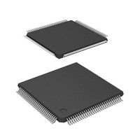
DF2398TE20 Renesas Electronics America, DF2398TE20 Datasheet - Page 656

DF2398TE20
Manufacturer Part Number
DF2398TE20
Description
IC H8S MCU FLASH 256K 120TQFP
Manufacturer
Renesas Electronics America
Series
H8® H8S/2300r
Specifications of DF2398TE20
Core Processor
H8S/2000
Core Size
16-Bit
Speed
20MHz
Connectivity
SCI, SmartCard
Peripherals
DMA, POR, PWM, WDT
Number Of I /o
87
Program Memory Size
256KB (256K x 8)
Program Memory Type
FLASH
Ram Size
8K x 8
Voltage - Supply (vcc/vdd)
4.5 V ~ 5.5 V
Data Converters
A/D 8x10b; D/A 2x8b
Oscillator Type
Internal
Operating Temperature
-20°C ~ 75°C
Package / Case
120-TQFP, 120-VQFP
Lead Free Status / RoHS Status
Contains lead / RoHS non-compliant
Eeprom Size
-
Other names
HD64F2398TE20
HD64F2398TE20
HD64F2398TE20
Available stocks
Company
Part Number
Manufacturer
Quantity
Price
Company:
Part Number:
DF2398TE20V
Manufacturer:
Renesas Electronics America
Quantity:
10 000
- Current page: 656 of 1049
- Download datasheet (5Mb)
19.15.8 Pin Configuration
The flash memory is controlled by means of the pins shown in table 19-31.
Table 19-31 Flash Memory Pins
19.15.9 Register Configuration
The registers used to control the on-chip flash memory when enabled are shown in table 19-32.
In order to access the FLMCR1, FLMCR2, EBR1, and EBR2 registers, the FLSHE bit must be set to 1 in SYSCR2
(except RAMER).
Table 19-32 Flash Memory Registers
Notes: 1. Lower 16 bits of the address.
Rev.6.00 Oct.28.2004 page 626 of 1016
REJ09B0138-0600H
2. Flash memory. Registers selection is performed by the FLSHE bit in system control register 2 (SYSCR2).
3. In modes in which the on-chip flash memory is disabled, a read will return H'00, and writes are invalid.
4. If a high level is input and the SWE bit in FLMCR1 is not set, these registers are initialized to H'00.
5. FLMCR1, FLMCR2, EBR1, and EBR2 are 8-bit registers. Only byte accesses are valid for these registers, the
6. The SYSCR2 register can only be used in the F-ZTAT version. In the masked ROM version this register will
access requiring 2 states.
return an undefined value if read, and cannot be modified.
Register Name
Flash memory control register 1
Flash memory control register 2
Erase block register 1
Erase block register 2
System control register 2
RAM emulation register
Pin Name
Reset
Mode 2
Mode 1
Mode 0
Port 66
Port 65
Port 64
Transmit data
Receive data
Abbreviation
RES
MD2
MD1
MD0
P66
P65
P64
TxD1
RxD1
I/O
Input
Input
Input
Input
Input
Input
Input
Output
Input
Abbreviation R/W
FLMCR1*
FLMCR2*
EBR1*
EBR2*
SYSCR2*
RAMER
5
5
Function
Reset
Sets MCU operating mode
Sets MCU operating mode
Sets MCU operating mode
Sets MCU operating mode in programmer mode
Sets MCU operating mode in programmer mode
Sets MCU operating mode in programmer mode
Serial transmit data output
Serial receive data input
5
5
6
R/W*
R/W*
R/W*
R/W*
R/W
R/W
3
3
3
3
Initial Value
H'80
H'00*
H'00*
H'00*
H'00
H'00
4
4
4
Address*
H'FFC8*
H'FFC9*
H'FFCA*
H'FFCB*
H'FF42
H'FEDB
2
2
2
2
1
Related parts for DF2398TE20
Image
Part Number
Description
Manufacturer
Datasheet
Request
R

Part Number:
Description:
CONN PLUG 12POS DUAL 0.5MM SMD
Manufacturer:
Hirose Electric Co Ltd
Datasheet:

Part Number:
Description:
CONN PLUG 18POS DUAL 0.5MM SMD
Manufacturer:
Hirose Electric Co Ltd
Datasheet:

Part Number:
Description:
CONN PLUG 14POS DUAL 0.5MM SMD
Manufacturer:
Hirose Electric Co Ltd
Datasheet:

Part Number:
Description:
CONN RECEPT 20POS DUAL 0.5MM SMD
Manufacturer:
Hirose Electric Co Ltd
Datasheet:

Part Number:
Description:
CONN PLUG 16POS DUAL 0.5MM SMD
Manufacturer:
Hirose Electric Co Ltd
Datasheet:

Part Number:
Description:
CONN RECEPT 16POS DUAL 0.5MM SMD
Manufacturer:
Hirose Electric Co Ltd
Datasheet:

Part Number:
Description:
CONN PLUG 20POS DUAL 0.5MM SMD
Manufacturer:
Hirose Electric Co Ltd
Datasheet:

Part Number:
Description:
CONN PLUG 30POS DUAL 0.5MM SMD
Manufacturer:
Hirose Electric Co Ltd
Datasheet:

Part Number:
Description:
CONN RECEPT 30POS DUAL 0.5MM SMD
Manufacturer:
Hirose Electric Co Ltd
Datasheet:

Part Number:
Description:
CONN PLUG 40POS DUAL 0.5MM SMD
Manufacturer:
Hirose Electric Co Ltd
Datasheet:

Part Number:
Description:
KIT STARTER FOR M16C/29
Manufacturer:
Renesas Electronics America
Datasheet:

Part Number:
Description:
KIT STARTER FOR R8C/2D
Manufacturer:
Renesas Electronics America
Datasheet:

Part Number:
Description:
R0K33062P STARTER KIT
Manufacturer:
Renesas Electronics America
Datasheet:

Part Number:
Description:
KIT STARTER FOR R8C/23 E8A
Manufacturer:
Renesas Electronics America
Datasheet:

Part Number:
Description:
KIT STARTER FOR R8C/25
Manufacturer:
Renesas Electronics America
Datasheet:


