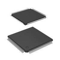
DF2398TE20 Renesas Electronics America, DF2398TE20 Datasheet - Page 625

DF2398TE20
Manufacturer Part Number
DF2398TE20
Description
IC H8S MCU FLASH 256K 120TQFP
Manufacturer
Renesas Electronics America
Series
H8® H8S/2300r
Specifications of DF2398TE20
Core Processor
H8S/2000
Core Size
16-Bit
Speed
20MHz
Connectivity
SCI, SmartCard
Peripherals
DMA, POR, PWM, WDT
Number Of I /o
87
Program Memory Size
256KB (256K x 8)
Program Memory Type
FLASH
Ram Size
8K x 8
Voltage - Supply (vcc/vdd)
4.5 V ~ 5.5 V
Data Converters
A/D 8x10b; D/A 2x8b
Oscillator Type
Internal
Operating Temperature
-20°C ~ 75°C
Package / Case
120-TQFP, 120-VQFP
Lead Free Status / RoHS Status
Contains lead / RoHS non-compliant
Eeprom Size
-
Other names
HD64F2398TE20
HD64F2398TE20
HD64F2398TE20
Available stocks
Company
Part Number
Manufacturer
Quantity
Price
Company:
Part Number:
DF2398TE20V
Manufacturer:
Renesas Electronics America
Quantity:
10 000
- Current page: 625 of 1049
- Download datasheet (5Mb)
19-19) and transferred to the reprogram data area. After 32 bytes of data have been verified, exit program-verify mode,
wait for at least ( ) s, then clear the SWE bit in FLMCR1 to 0. If reprogramming is necessary, set program mode again,
and repeat the program/program-verify sequence as before. However, ensure that the program/program-verify sequence is
not repeated more than (N) times on the same bits.
Increment address
NG
Write 32-byte data in RAM reprogram data
Store 32-byte program data in program
Transfer reprogram data to reprogram
data area and reprogram data area
H'FF dummy write to verify address
area consecutively to flash memory
Reprogram data computation
Figure 19-19 Program/Program-Verify Flowchart
Clear SWE bit in FLMCR1
Clear PSU bit in FLMCR2
Set SWE bit in FLMCR1
Clear PV bit in FLMCR1
Set PSU bit in FLMCR2
Clear P bit in FLMCR1
Set PV bit in FLMCR1
Set P bit in FLMCR1
End of programming
Read verify data
data verification?
Program data =
End of 32-byte
Disable WDT
Enable WDT
Wait (x) s
Wait (y) s
Wait (z) s
Wait ( ) s
Wait ( ) s
Wait ( ) s
Wait ( ) s
Wait ( ) s
verify data?
OK
data area
m = 0?
m = 0
n = 1
Start
OK
OK
*3
NG
NG
*5
*4
*1
*5
Start of programming
*5
End of programming
*5
*5
*5
*5
*2
*3
*4
*5
m = 1
Notes: 1. Data transfer is performed by byte transfer. The lower
Clear SWE bit in FLMCR1
Programming failure
2. Verify data is read in 16-bit (word) units.
3. Even bits for which programming has been completed in a 32-byte
4. An area for storing program data (32 bytes) and reprogram data
5. The values of x, y, z, , , , , , and N are shown in section
Program
Data
Note: The memory erased state is 1. Programming is
0
0
1
1
8 bits of the first address written to must be H'00, H'20, H'40,
H'60, H'80, H'A0, H'C0, or H'E0. A 32-byte data transfer
must be performed even if writing fewer than 32 bytes;
in this case, H'FF data must be written to the extra addresses.
programming loop will be subjected to additional programming if
the subsequent verify operation fails.
(32 bytes) must be provided in RAM. The contents of the latter
are rewritten as programming progresses.
22.7.6, Flash Memory Characteristics.
n
Perform programming in the erased state.
Do not perform additional programming
on previously programmed addresses.
performed on 0 reprogram data.
N?
Verify
Data
0
1
0
1
OK
*5
Reprogram
Data
1
0
1
1
NG
n
Rev.6.00 Oct.28.2004 page 595 of 1016
n + 1
Comments
Programmed bits are
not reprogrammed
Programming incomplete;
reprogram
—
Still in erased state;
no action
Reprogram data storage
Program data storage
area (32 bytes)
area (32 bytes)
RAM
REJ09B0138-0600H
Related parts for DF2398TE20
Image
Part Number
Description
Manufacturer
Datasheet
Request
R

Part Number:
Description:
CONN PLUG 12POS DUAL 0.5MM SMD
Manufacturer:
Hirose Electric Co Ltd
Datasheet:

Part Number:
Description:
CONN PLUG 18POS DUAL 0.5MM SMD
Manufacturer:
Hirose Electric Co Ltd
Datasheet:

Part Number:
Description:
CONN PLUG 14POS DUAL 0.5MM SMD
Manufacturer:
Hirose Electric Co Ltd
Datasheet:

Part Number:
Description:
CONN RECEPT 20POS DUAL 0.5MM SMD
Manufacturer:
Hirose Electric Co Ltd
Datasheet:

Part Number:
Description:
CONN PLUG 16POS DUAL 0.5MM SMD
Manufacturer:
Hirose Electric Co Ltd
Datasheet:

Part Number:
Description:
CONN RECEPT 16POS DUAL 0.5MM SMD
Manufacturer:
Hirose Electric Co Ltd
Datasheet:

Part Number:
Description:
CONN PLUG 20POS DUAL 0.5MM SMD
Manufacturer:
Hirose Electric Co Ltd
Datasheet:

Part Number:
Description:
CONN PLUG 30POS DUAL 0.5MM SMD
Manufacturer:
Hirose Electric Co Ltd
Datasheet:

Part Number:
Description:
CONN RECEPT 30POS DUAL 0.5MM SMD
Manufacturer:
Hirose Electric Co Ltd
Datasheet:

Part Number:
Description:
CONN PLUG 40POS DUAL 0.5MM SMD
Manufacturer:
Hirose Electric Co Ltd
Datasheet:

Part Number:
Description:
KIT STARTER FOR M16C/29
Manufacturer:
Renesas Electronics America
Datasheet:

Part Number:
Description:
KIT STARTER FOR R8C/2D
Manufacturer:
Renesas Electronics America
Datasheet:

Part Number:
Description:
R0K33062P STARTER KIT
Manufacturer:
Renesas Electronics America
Datasheet:

Part Number:
Description:
KIT STARTER FOR R8C/23 E8A
Manufacturer:
Renesas Electronics America
Datasheet:

Part Number:
Description:
KIT STARTER FOR R8C/25
Manufacturer:
Renesas Electronics America
Datasheet:


