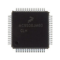
MC9S08JM60CLH Freescale, MC9S08JM60CLH Datasheet - Page 136

MC9S08JM60CLH
Manufacturer Part Number
MC9S08JM60CLH
Description
Manufacturer
Freescale
Datasheet
1.MC9S08JM60CLH.pdf
(388 pages)
Specifications of MC9S08JM60CLH
Cpu Family
HCS08
Device Core Size
8b
Frequency (max)
24MHz
Interface Type
SCI/SPI
Total Internal Ram Size
4KB
# I/os (max)
51
Number Of Timers - General Purpose
8
Operating Supply Voltage (typ)
3.3/5V
Operating Supply Voltage (max)
5.5V
Operating Supply Voltage (min)
2.7V
On-chip Adc
12-chx12-bit
Instruction Set Architecture
CISC
Operating Temp Range
-40C to 85C
Operating Temperature Classification
Industrial
Mounting
Surface Mount
Pin Count
64
Package Type
LQFP
Program Memory Type
Flash
Program Memory Size
60KB
Lead Free Status / RoHS Status
Compliant
Available stocks
Company
Part Number
Manufacturer
Quantity
Price
Company:
Part Number:
MC9S08JM60CLH
Manufacturer:
Freescale Semiconductor
Quantity:
10 000
Part Number:
MC9S08JM60CLH
Manufacturer:
FREESCALE
Quantity:
20 000
Company:
Part Number:
MC9S08JM60CLHE
Manufacturer:
AZBIL
Quantity:
1 000
- Current page: 136 of 388
- Download datasheet (5Mb)
Chapter 10 Analog-to-Digital Converter (S08ADC12V1)
10.1.1.2
The ADC is capable of performing conversions using the MCU bus clock, the bus clock divided by two,
the local asynchronous clock (ADACK) within the module, or the alternate clock (ALTCLK). The
ALTCLK on this device is the MCGERCLK.
The selected clock source must run at a frequency such that the ADC conversion clock (ADCK) runs at a
frequency within its specified range (f
determined by the ADIV bits.
ALTCLK is active while the MCU is in wait mode provided the conditions described above are met. This
allows ALTCLK to be used as the conversion clock source for the ADC while the MCU is in wait mode.
ALTCLK cannot be used as the ADC conversion clock source while the MCU is in stop3.
10.1.1.3
The RTC on this device can be enabled as a hardware trigger for the ADC module by setting the
136
1
ADCH
00000
00001
00010
00011
00100
00101
00110
00111
01000
01001
01010
01011
01100
01101
01110
01111
For more information, see
Channel
AD10
AD11
AD12
AD13
AD14
AD15
AD0
AD1
AD2
AD3
AD4
AD5
AD6
AD7
AD8
AD9
Alternate Clock
Hardware Trigger
Selecting the internal bandgap channel requires BGBE =1 in SPMSC1 see
Section 5.7.7, “System Power Management Status and Control 1 Register
(SPMSC1).” For value of bandgap voltage reference see
“Analog Comparator (ACMP)
PTB2/SPSCK2/ADP2
PTD0/ADP8/ACMP+
PTD3/KBIP3/ADP10
PTD1/ADP9/ACMP-
PTB0/MISO2/ADP0
PTB1/MOSI2/ADP1
PTB4/KBIP4/ADP4
PTB5/KBIP5/ADP5
PTB3/SS2/ADP3
PTD4/ADP11
Section 10.1.1.5, “Temperature
PTB6/ADP6
PTB7/ADP7
V
V
V
V
Input
REFL
REFL
REFL
REFL
Table 10-1. ADC Channel Assignment
MC9S08JM60 Series Data Sheet, Rev. 3
ADCK
Pin Control
ADPC10
ADPC11
ADPC12
ADPC13
ADPC14
ADPC15
) after being divided down from the ALTCLK input as
ADPC0
ADPC1
ADPC2
ADPC3
ADPC4
ADPC5
ADPC6
ADPC7
ADPC8
ADPC9
Electricals.”
NOTE
Sensor.”
ADCH
10000
10001
10010
10011
10100
10101
10110
10111
11000
11001
11010
11011
11100
11101
11110
11111
Channel
disabled
module
V
V
AD16
AD17
AD18
AD19
AD20
AD21
AD22
AD23
AD24
AD25
AD26
AD27
REFH
REFL
Appendix A.8,
Internal Bandgap
Temperature
Reserved
Reserved
Reserved
Reserved
Reserved
Reserved
Sensor
V
V
V
V
V
V
V
Input
None
REFH
REFL
REFL
REFL
REFL
REFL
REFL
Freescale Semiconductor
1
Pin Control
N/A
N/A
N/A
N/A
N/A
N/A
N/A
N/A
N/A
N/A
N/A
N/A
N/A
N/A
N/A
N/A
Related parts for MC9S08JM60CLH
Image
Part Number
Description
Manufacturer
Datasheet
Request
R

Part Number:
Description:
TOWER ELEVATOR BOARDS HARDWARE
Manufacturer:
Freescale Semiconductor
Datasheet:

Part Number:
Description:
TOWER SERIAL I/O HARDWARE
Manufacturer:
Freescale Semiconductor
Datasheet:

Part Number:
Description:
LCD MODULE FOR TWR SYSTEM
Manufacturer:
Freescale Semiconductor
Datasheet:

Part Number:
Description:
DAUGHTER LCD WVGA I.MX51
Manufacturer:
Freescale Semiconductor
Datasheet:

Part Number:
Description:
TOWER SYSTEM BOARD MPC5125
Manufacturer:
Freescale Semiconductor
Datasheet:

Part Number:
Description:
KIT EVALUATION I.MX51
Manufacturer:
Freescale Semiconductor
Datasheet:

Part Number:
Description:
KIT DEVELOPMENT WINCE IMX25
Manufacturer:
Freescale Semiconductor
Datasheet:

Part Number:
Description:
TOWER SYSTEM KIT MPC5125
Manufacturer:
Freescale Semiconductor
Datasheet:

Part Number:
Description:
TOWER SYSTEM BOARD K40X256
Manufacturer:
Freescale Semiconductor
Datasheet:

Part Number:
Description:
TOWER SYSTEM KIT K40X256
Manufacturer:
Freescale Semiconductor
Datasheet:

Part Number:
Description:
Microcontrollers (MCU) MX28 PLATFORM DEV KIT
Manufacturer:
Freescale Semiconductor
Datasheet:

Part Number:
Description:
MCU, MPU & DSP Development Tools IAR KickStart Kit for Kinetis K60
Manufacturer:
Freescale Semiconductor
Datasheet:

Part Number:
Description:
24BIT HDMI MX535/08
Manufacturer:
Freescale Semiconductor
Datasheet:
Part Number:
Description:
Manufacturer:
Freescale Semiconductor, Inc
Datasheet:
Part Number:
Description:
Manufacturer:
Freescale Semiconductor, Inc
Datasheet:


