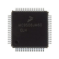
MC9S08JM60CLH Freescale, MC9S08JM60CLH Datasheet - Page 83

MC9S08JM60CLH
Manufacturer Part Number
MC9S08JM60CLH
Description
Manufacturer
Freescale
Datasheet
1.MC9S08JM60CLH.pdf
(388 pages)
Specifications of MC9S08JM60CLH
Cpu Family
HCS08
Device Core Size
8b
Frequency (max)
24MHz
Interface Type
SCI/SPI
Total Internal Ram Size
4KB
# I/os (max)
51
Number Of Timers - General Purpose
8
Operating Supply Voltage (typ)
3.3/5V
Operating Supply Voltage (max)
5.5V
Operating Supply Voltage (min)
2.7V
On-chip Adc
12-chx12-bit
Instruction Set Architecture
CISC
Operating Temp Range
-40C to 85C
Operating Temperature Classification
Industrial
Mounting
Surface Mount
Pin Count
64
Package Type
LQFP
Program Memory Type
Flash
Program Memory Size
60KB
Lead Free Status / RoHS Status
Compliant
Available stocks
Company
Part Number
Manufacturer
Quantity
Price
Company:
Part Number:
MC9S08JM60CLH
Manufacturer:
Freescale Semiconductor
Quantity:
10 000
Part Number:
MC9S08JM60CLH
Manufacturer:
FREESCALE
Quantity:
20 000
Company:
Part Number:
MC9S08JM60CLHE
Manufacturer:
AZBIL
Quantity:
1 000
- Current page: 83 of 388
- Download datasheet (5Mb)
6.3.1
An internal pullup device can be enabled for each port pin by setting the corresponding bit in one of the
pullup enable registers (PTxPEn). The pullup device is disabled if the pin is configured as an output by the
parallel I/O control logic or any shared peripheral function regardless of the state of the corresponding
pullup enable register bit. The pullup device is also disabled if the pin is controlled by an analog function.
6.3.2
Slew rate control can be enabled for each port pin by setting the corresponding bit in one of the slew rate
control registers (PTxSEn). When enabled, slew control limits the rate at which an output can transition in
order to reduce EMC emissions. Slew rate control has no effect on pins which are configured as inputs.
6.3.3
An output pin can be selected to have high output drive strength by setting the corresponding bit in one of
the drive strength select registers (PTxDSn). When high drive is selected a pin is capable of sourcing and
sinking greater current. Even though every I/O pin can be selected as high drive, the user must ensure that
the total current source and sink limits for the chip are not exceeded. Drive strength selection is intended
to affect the DC behavior of I/O pins. However, the AC behavior is also affected. High drive allows a pin
to drive a greater load with the same switching speed as a low drive enabled pin into a smaller load.
Because of this the EMC emissions may be affected by enabling pins as high drive.
6.4
Depending on the stop mode, I/O functions differently as the result of executing a STOP instruction. An
explanation of I/O behavior for the various stop modes follows:
6.5
This section provides information about the registers associated with the parallel I/O ports and pin control
functions. These parallel I/O registers are located in page zero of the memory map and the pin control
registers are located in the high page register section of memory.
Freescale Semiconductor
•
•
Stop2 mode is a partial power-down mode, whereby I/O latches are maintained in their state as
before the STOP instruction was executed. CPU register status and the state of I/O registers must
be saved in RAM before the STOP instruction is executed to place the MCU in stop2 mode. Upon
recovery from stop2 mode, before accessing any I/O, the user must examine the state of the PPDF
bit in the SPMSC2 register. If the PPDF bit is 0, I/O must be initialized as if a power on reset had
occurred. If the PPDF bit is 1, I/O data previously stored in RAM, before the STOP instruction was
executed, peripherals may require being initialized and restored to their pre-stop condition. The
user must then write a 1 to the PPDACK bit in the SPMSC2 register. Access to I/O is now permitted
again in the user’s application program.
In stop3 mode, all I/O is maintained because internal logic circuity stays powered up. Upon
recovery, normal I/O function is available to the user.
Pin Behavior in Stop Modes
Parallel I/O and Pin Control Registers
Internal Pullup Enable
Output Slew Rate Control Enable
Output Drive Strength Select
MC9S08JM60 Series Data Sheet, Rev. 3
Chapter 6 Parallel Input/Output
83
Related parts for MC9S08JM60CLH
Image
Part Number
Description
Manufacturer
Datasheet
Request
R

Part Number:
Description:
TOWER ELEVATOR BOARDS HARDWARE
Manufacturer:
Freescale Semiconductor
Datasheet:

Part Number:
Description:
TOWER SERIAL I/O HARDWARE
Manufacturer:
Freescale Semiconductor
Datasheet:

Part Number:
Description:
LCD MODULE FOR TWR SYSTEM
Manufacturer:
Freescale Semiconductor
Datasheet:

Part Number:
Description:
DAUGHTER LCD WVGA I.MX51
Manufacturer:
Freescale Semiconductor
Datasheet:

Part Number:
Description:
TOWER SYSTEM BOARD MPC5125
Manufacturer:
Freescale Semiconductor
Datasheet:

Part Number:
Description:
KIT EVALUATION I.MX51
Manufacturer:
Freescale Semiconductor
Datasheet:

Part Number:
Description:
KIT DEVELOPMENT WINCE IMX25
Manufacturer:
Freescale Semiconductor
Datasheet:

Part Number:
Description:
TOWER SYSTEM KIT MPC5125
Manufacturer:
Freescale Semiconductor
Datasheet:

Part Number:
Description:
TOWER SYSTEM BOARD K40X256
Manufacturer:
Freescale Semiconductor
Datasheet:

Part Number:
Description:
TOWER SYSTEM KIT K40X256
Manufacturer:
Freescale Semiconductor
Datasheet:

Part Number:
Description:
Microcontrollers (MCU) MX28 PLATFORM DEV KIT
Manufacturer:
Freescale Semiconductor
Datasheet:

Part Number:
Description:
MCU, MPU & DSP Development Tools IAR KickStart Kit for Kinetis K60
Manufacturer:
Freescale Semiconductor
Datasheet:

Part Number:
Description:
24BIT HDMI MX535/08
Manufacturer:
Freescale Semiconductor
Datasheet:
Part Number:
Description:
Manufacturer:
Freescale Semiconductor, Inc
Datasheet:
Part Number:
Description:
Manufacturer:
Freescale Semiconductor, Inc
Datasheet:


