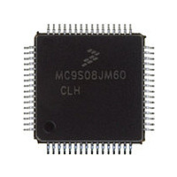
MC9S08JM60CLH Freescale, MC9S08JM60CLH Datasheet - Page 318

MC9S08JM60CLH
Manufacturer Part Number
MC9S08JM60CLH
Description
Manufacturer
Freescale
Datasheet
1.MC9S08JM60CLH.pdf
(388 pages)
Specifications of MC9S08JM60CLH
Cpu Family
HCS08
Device Core Size
8b
Frequency (max)
24MHz
Interface Type
SCI/SPI
Total Internal Ram Size
4KB
# I/os (max)
51
Number Of Timers - General Purpose
8
Operating Supply Voltage (typ)
3.3/5V
Operating Supply Voltage (max)
5.5V
Operating Supply Voltage (min)
2.7V
On-chip Adc
12-chx12-bit
Instruction Set Architecture
CISC
Operating Temp Range
-40C to 85C
Operating Temperature Classification
Industrial
Mounting
Surface Mount
Pin Count
64
Package Type
LQFP
Program Memory Type
Flash
Program Memory Size
60KB
Lead Free Status / RoHS Status
Compliant
Available stocks
Company
Part Number
Manufacturer
Quantity
Price
Company:
Part Number:
MC9S08JM60CLH
Manufacturer:
Freescale Semiconductor
Quantity:
10 000
Part Number:
MC9S08JM60CLH
Manufacturer:
FREESCALE
Quantity:
20 000
Company:
Part Number:
MC9S08JM60CLHE
Manufacturer:
AZBIL
Quantity:
1 000
- Current page: 318 of 388
- Download datasheet (5Mb)
Universal Serial Bus Device Controller (S08USBV1)
The BDT is composed of buffer descriptors (BD) which are used to define and control the actual buffers
in the USB RAM space. BDs always occur as a 3-bytes block. See
Endpoint 0 IN start from USB RAM offset 0x00.
The format for the buffer descriptor is shown in
318
BDTKPID[3:0]
0x00
0x01
0x02
BDTSTALL
DATA0/1
•
•
OWN
Offset
Field
DTS
How much data was transmitted or received.
Where the buffer resides in buffer memory
W
W
W
R
R
R
OWN — This OWN bit determines who currently owns the buffer. The USB SIE generally writes a 0 to this bit
when it has completed a token. The USB module ignores all other fields in the BD when OWN=0. Once the BD
has been assigned to the USB module (OWN=1), the MCU must not change it in any way. This byte of the BD
must always be the last byte the MCU (firmware) updates when it initializes a BD. Although the hardware will
not block the MCU from accessing the BD while owned by the USB SIE, doing so may cause undefined
behavior and is generally not recommended.
0 The MCU has exclusive access to the entire BD
1 The USB module has exclusive access to the BD
Data Toggle — This bit defines if a DATA0 field (DATA0/1=0) or a DATA1 (DATA0/1=1) field was transmitted or
received. It is unchanged by the USB module.
0 Data 0 packet
1 Data 1 packet
The current token PID is written back to the BD by the USB module when a transfer completes. The values
written back are the token PID values from the USB specification: 0x1 for an OUT token, 0x9 for and IN token
or 0xd for a SETUP token.
Data Toggle Synchronization— This bit enables data toggle synchronization.
0 No data toggle synchronization is performed.
1 Data toggle synchronization is performed.
BDT Stall — Setting this bit will cause the USB module to issue a STALL handshake if a token is received by
the SIE that would use the BDT in this location. The BDT is not consumed by the SIE (the OWN bit remains
and the rest of the BD is unchanged) when the BDTSTALL bit is set.
0 BDT stall is disabled
1 USB will issue a STALL handshake if a token is received by the SIE that would use the BDT in this location
OWN
7
DATA0/1
6
Table 17-22. Buffer Descriptor Table Fields
Figure 17-19. Buffer Descriptor Example
MC9S08JM60 Series Data Sheet, Rev. 3
BDTKPID[3] BDTKPID[3] BDTKPID[1] BDTKPID[0]
5
0
EPADR[9:4]
Table
4
0
Description
17-22.
BC[7:0]
DTS
3
Figure 17-19
BDTSTALL
2
for the BD example of
Freescale Semiconductor
1
0
0
0
Related parts for MC9S08JM60CLH
Image
Part Number
Description
Manufacturer
Datasheet
Request
R

Part Number:
Description:
TOWER ELEVATOR BOARDS HARDWARE
Manufacturer:
Freescale Semiconductor
Datasheet:

Part Number:
Description:
TOWER SERIAL I/O HARDWARE
Manufacturer:
Freescale Semiconductor
Datasheet:

Part Number:
Description:
LCD MODULE FOR TWR SYSTEM
Manufacturer:
Freescale Semiconductor
Datasheet:

Part Number:
Description:
DAUGHTER LCD WVGA I.MX51
Manufacturer:
Freescale Semiconductor
Datasheet:

Part Number:
Description:
TOWER SYSTEM BOARD MPC5125
Manufacturer:
Freescale Semiconductor
Datasheet:

Part Number:
Description:
KIT EVALUATION I.MX51
Manufacturer:
Freescale Semiconductor
Datasheet:

Part Number:
Description:
KIT DEVELOPMENT WINCE IMX25
Manufacturer:
Freescale Semiconductor
Datasheet:

Part Number:
Description:
TOWER SYSTEM KIT MPC5125
Manufacturer:
Freescale Semiconductor
Datasheet:

Part Number:
Description:
TOWER SYSTEM BOARD K40X256
Manufacturer:
Freescale Semiconductor
Datasheet:

Part Number:
Description:
TOWER SYSTEM KIT K40X256
Manufacturer:
Freescale Semiconductor
Datasheet:

Part Number:
Description:
Microcontrollers (MCU) MX28 PLATFORM DEV KIT
Manufacturer:
Freescale Semiconductor
Datasheet:

Part Number:
Description:
MCU, MPU & DSP Development Tools IAR KickStart Kit for Kinetis K60
Manufacturer:
Freescale Semiconductor
Datasheet:

Part Number:
Description:
24BIT HDMI MX535/08
Manufacturer:
Freescale Semiconductor
Datasheet:
Part Number:
Description:
Manufacturer:
Freescale Semiconductor, Inc
Datasheet:
Part Number:
Description:
Manufacturer:
Freescale Semiconductor, Inc
Datasheet:


