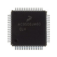
MC9S08JM60CLH Freescale, MC9S08JM60CLH Datasheet - Page 286

MC9S08JM60CLH
Manufacturer Part Number
MC9S08JM60CLH
Description
Manufacturer
Freescale
Datasheet
1.MC9S08JM60CLH.pdf
(388 pages)
Specifications of MC9S08JM60CLH
Cpu Family
HCS08
Device Core Size
8b
Frequency (max)
24MHz
Interface Type
SCI/SPI
Total Internal Ram Size
4KB
# I/os (max)
51
Number Of Timers - General Purpose
8
Operating Supply Voltage (typ)
3.3/5V
Operating Supply Voltage (max)
5.5V
Operating Supply Voltage (min)
2.7V
On-chip Adc
12-chx12-bit
Instruction Set Architecture
CISC
Operating Temp Range
-40C to 85C
Operating Temperature Classification
Industrial
Mounting
Surface Mount
Pin Count
64
Package Type
LQFP
Program Memory Type
Flash
Program Memory Size
60KB
Lead Free Status / RoHS Status
Compliant
Available stocks
Company
Part Number
Manufacturer
Quantity
Price
Company:
Part Number:
MC9S08JM60CLH
Manufacturer:
Freescale Semiconductor
Quantity:
10 000
Part Number:
MC9S08JM60CLH
Manufacturer:
FREESCALE
Quantity:
20 000
Company:
Part Number:
MC9S08JM60CLHE
Manufacturer:
AZBIL
Quantity:
1 000
- Current page: 286 of 388
- Download datasheet (5Mb)
Timer/PWM Module (S08TPMV3)
In input capture mode, reading either byte (TPMxCnVH or TPMxCnVL) latches the contents of both bytes
into a buffer where they remain latched until the other half is read. This latching mechanism also resets
(becomes unlatched) when the TPMxCnSC register is written (whether BDM mode is active or not). Any
write to the channel registers will be ignored during the input capture mode.
When BDM is active, the coherency mechanism is frozen (unless reset by writing to TPMxCnSC register)
such that the buffer latches remain in the state they were in when the BDM became active, even if one or
both halves of the channel register are read while BDM is active. This assures that if the user was in the
middle of reading a 16-bit register when BDM became active, it will read the appropriate value from the
other half of the 16-bit value after returning to normal execution. The value read from the TPMxCnVH
and TPMxCnVL registers in BDM mode is the value of these registers and not the value of their read
buffer.
In output compare or PWM modes, writing to either byte (TPMxCnVH or TPMxCnVL) latches the value
into a buffer. After both bytes are written, they are transferred as a coherent 16-bit value into the
timer-channel registers according to the value of CLKSB:CLKSA bits and the selected mode, so:
The latching mechanism may be manually reset by writing to the TPMxCnSC register (whether BDM
mode is active or not). This latching mechanism allows coherent 16-bit writes in either big-endian or
little-endian order which is friendly to various compiler implementations.
When BDM is active, the coherency mechanism is frozen such that the buffer latches remain in the state
they were in when the BDM became active even if one or both halves of the channel register are written
while BDM is active. Any write to the channel registers bypasses the buffer latches and directly write to
the channel register while BDM is active. The values written to the channel register while BDM is active
are used for PWM & output compare operation once normal execution resumes. Writes to the channel
registers while BDM is active do not interfere with partial completion of a coherency sequence. After the
coherency mechanism has been fully exercised, the channel registers are updated using the buffered values
written (while BDM was not active) by the user.
16.4
All TPM functions are associated with a central 16-bit counter which allows flexible selection of the clock
source and prescale factor. There is also a 16-bit modulo register associated with the main counter.
The CPWMS control bit chooses between center-aligned PWM operation for all channels in the TPM
(CPWMS=1) or general purpose timing functions (CPWMS=0) where each channel can independently be
configured to operate in input capture, output compare, or edge-aligned PWM mode. The CPWMS control
bit is located in the main TPM status and control register because it affects all channels within the TPM
286
•
•
•
If (CLKSB:CLKSA = 0:0), then the registers are updated when the second byte is written.
If (CLKSB:CLKSA not = 0:0 and in output compare mode) then the registers are updated after the
second byte is written and on the next change of the TPM counter (end of the prescaler counting).
If (CLKSB:CLKSA not = 0:0 and in EPWM or CPWM modes), then the registers are updated after
the both bytes were written, and the TPM counter changes from (TPMxMODH:TPMxMODL - 1)
to (TPMxMODH:TPMxMODL). If the TPM counter is a free-running counter then the update is
made when the TPM counter changes from 0xFFFE to 0xFFFF.
Functional Description
MC9S08JM60 Series Data Sheet, Rev. 3
Freescale Semiconductor
Related parts for MC9S08JM60CLH
Image
Part Number
Description
Manufacturer
Datasheet
Request
R

Part Number:
Description:
TOWER ELEVATOR BOARDS HARDWARE
Manufacturer:
Freescale Semiconductor
Datasheet:

Part Number:
Description:
TOWER SERIAL I/O HARDWARE
Manufacturer:
Freescale Semiconductor
Datasheet:

Part Number:
Description:
LCD MODULE FOR TWR SYSTEM
Manufacturer:
Freescale Semiconductor
Datasheet:

Part Number:
Description:
DAUGHTER LCD WVGA I.MX51
Manufacturer:
Freescale Semiconductor
Datasheet:

Part Number:
Description:
TOWER SYSTEM BOARD MPC5125
Manufacturer:
Freescale Semiconductor
Datasheet:

Part Number:
Description:
KIT EVALUATION I.MX51
Manufacturer:
Freescale Semiconductor
Datasheet:

Part Number:
Description:
KIT DEVELOPMENT WINCE IMX25
Manufacturer:
Freescale Semiconductor
Datasheet:

Part Number:
Description:
TOWER SYSTEM KIT MPC5125
Manufacturer:
Freescale Semiconductor
Datasheet:

Part Number:
Description:
TOWER SYSTEM BOARD K40X256
Manufacturer:
Freescale Semiconductor
Datasheet:

Part Number:
Description:
TOWER SYSTEM KIT K40X256
Manufacturer:
Freescale Semiconductor
Datasheet:

Part Number:
Description:
Microcontrollers (MCU) MX28 PLATFORM DEV KIT
Manufacturer:
Freescale Semiconductor
Datasheet:

Part Number:
Description:
MCU, MPU & DSP Development Tools IAR KickStart Kit for Kinetis K60
Manufacturer:
Freescale Semiconductor
Datasheet:

Part Number:
Description:
24BIT HDMI MX535/08
Manufacturer:
Freescale Semiconductor
Datasheet:
Part Number:
Description:
Manufacturer:
Freescale Semiconductor, Inc
Datasheet:
Part Number:
Description:
Manufacturer:
Freescale Semiconductor, Inc
Datasheet:


