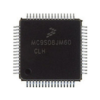
MC9S08JM60CLH Freescale, MC9S08JM60CLH Datasheet - Page 37

MC9S08JM60CLH
Manufacturer Part Number
MC9S08JM60CLH
Description
Manufacturer
Freescale
Datasheet
1.MC9S08JM60CLH.pdf
(388 pages)
Specifications of MC9S08JM60CLH
Cpu Family
HCS08
Device Core Size
8b
Frequency (max)
24MHz
Interface Type
SCI/SPI
Total Internal Ram Size
4KB
# I/os (max)
51
Number Of Timers - General Purpose
8
Operating Supply Voltage (typ)
3.3/5V
Operating Supply Voltage (max)
5.5V
Operating Supply Voltage (min)
2.7V
On-chip Adc
12-chx12-bit
Instruction Set Architecture
CISC
Operating Temp Range
-40C to 85C
Operating Temperature Classification
Industrial
Mounting
Surface Mount
Pin Count
64
Package Type
LQFP
Program Memory Type
Flash
Program Memory Size
60KB
Lead Free Status / RoHS Status
Compliant
Available stocks
Company
Part Number
Manufacturer
Quantity
Price
Company:
Part Number:
MC9S08JM60CLH
Manufacturer:
Freescale Semiconductor
Quantity:
10 000
Part Number:
MC9S08JM60CLH
Manufacturer:
FREESCALE
Quantity:
20 000
Company:
Part Number:
MC9S08JM60CLHE
Manufacturer:
AZBIL
Quantity:
1 000
- Current page: 37 of 388
- Download datasheet (5Mb)
3.6
One of two stop modes is entered upon execution of a STOP instruction when STOPE in SOPT1 is set. In
any stop mode, the bus and CPU clocks are halted. The MCG module can be configured to leave the
reference clocks running. See
information.
Table 3-1
conditions. The selected mode is entered following the execution of a STOP instruction.
3.6.1
Stop3 mode is entered by executing a STOP instruction under the conditions as shown in
states of all of the internal registers and logic, RAM contents, and I/O pin states are maintained.
Stop3 can be exited by asserting RESET, or by an interrupt from one of the following sources: the real-time
clock (RTC) interrupt, the USB resume interrupt, LVD, ADC, IRQ, KBI, SCI, or the ACMP.
If stop3 is exited by means of the RESET pin, then the MCU is reset and operation will resume after taking
the reset vector. Exit by means of one of the internal interrupt sources results in the MCU taking the
appropriate interrupt vector.
3.6.1.1
The LVD system is capable of generating either an interrupt or a reset when the supply voltage drops below
the LVD voltage. If the LVD is enabled in stop (LVDE and LVDSE bits in SPMSC1 both set) at the time
the CPU executes a STOP instruction, then the voltage regulator remains active during stop mode. If the
user attempts to enter stop2 with the LVD enabled for stop, the MCU will enter stop3 instead.
For the ADC to operate, the LVD must be left enabled when entering stop3. For the ACMP to operate when
ACGBS in ACMPSC is set, the LVD must be left enabled when entering stop3.
For the XOSC to operate with an external reference when RANGE in MCGC2 is set, the LVD must be left
enabled when entering stop3.
Freescale Semiconductor
1
2
STOPE
Stop Modes
ENBDM is located in the BDCSCR which is only accessible through BDC commands, see
“BDC Status and Control Register
When in stop3 mode with BDM enabled, The S
enabled.
shows all of the control bits that affect stop mode selection and the mode selected under various
0
1
1
1
1
Stop3 Mode
LVD Enabled in Stop Mode
ENBDM
x
1
0
0
0
1
Both bits must be 1
LVDE
Chapter 12, “Multi-Purpose Clock Generator
Either bit a 0
Either bit a 0
MC9S08JM60 Series Data Sheet, Rev. 3
x
x
Table 3-1. Stop Mode Selection
LVDSE
(BDCSCR).”
PPDC
0
1
x
x
x
IDD
will be near R
Stop modes disabled; illegal opcode reset if STOP
instruction executed
Stop3 with BDM enabled
Stop3 with voltage regulator active
Stop3
Stop2
IDD
levels because internal clocks are
Stop Mode
2
(S08MCGV1),” for more
Chapter 3 Modes of Operation
Section 18.4.1.1,
Table
3-1. The
37
Related parts for MC9S08JM60CLH
Image
Part Number
Description
Manufacturer
Datasheet
Request
R

Part Number:
Description:
TOWER ELEVATOR BOARDS HARDWARE
Manufacturer:
Freescale Semiconductor
Datasheet:

Part Number:
Description:
TOWER SERIAL I/O HARDWARE
Manufacturer:
Freescale Semiconductor
Datasheet:

Part Number:
Description:
LCD MODULE FOR TWR SYSTEM
Manufacturer:
Freescale Semiconductor
Datasheet:

Part Number:
Description:
DAUGHTER LCD WVGA I.MX51
Manufacturer:
Freescale Semiconductor
Datasheet:

Part Number:
Description:
TOWER SYSTEM BOARD MPC5125
Manufacturer:
Freescale Semiconductor
Datasheet:

Part Number:
Description:
KIT EVALUATION I.MX51
Manufacturer:
Freescale Semiconductor
Datasheet:

Part Number:
Description:
KIT DEVELOPMENT WINCE IMX25
Manufacturer:
Freescale Semiconductor
Datasheet:

Part Number:
Description:
TOWER SYSTEM KIT MPC5125
Manufacturer:
Freescale Semiconductor
Datasheet:

Part Number:
Description:
TOWER SYSTEM BOARD K40X256
Manufacturer:
Freescale Semiconductor
Datasheet:

Part Number:
Description:
TOWER SYSTEM KIT K40X256
Manufacturer:
Freescale Semiconductor
Datasheet:

Part Number:
Description:
Microcontrollers (MCU) MX28 PLATFORM DEV KIT
Manufacturer:
Freescale Semiconductor
Datasheet:

Part Number:
Description:
MCU, MPU & DSP Development Tools IAR KickStart Kit for Kinetis K60
Manufacturer:
Freescale Semiconductor
Datasheet:

Part Number:
Description:
24BIT HDMI MX535/08
Manufacturer:
Freescale Semiconductor
Datasheet:
Part Number:
Description:
Manufacturer:
Freescale Semiconductor, Inc
Datasheet:
Part Number:
Description:
Manufacturer:
Freescale Semiconductor, Inc
Datasheet:


