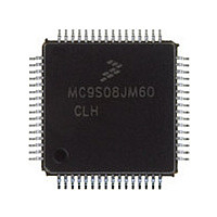
MC9S08JM60CLH Freescale, MC9S08JM60CLH Datasheet - Page 187

MC9S08JM60CLH
Manufacturer Part Number
MC9S08JM60CLH
Description
Manufacturer
Freescale
Datasheet
1.MC9S08JM60CLH.pdf
(388 pages)
Specifications of MC9S08JM60CLH
Cpu Family
HCS08
Device Core Size
8b
Frequency (max)
24MHz
Interface Type
SCI/SPI
Total Internal Ram Size
4KB
# I/os (max)
51
Number Of Timers - General Purpose
8
Operating Supply Voltage (typ)
3.3/5V
Operating Supply Voltage (max)
5.5V
Operating Supply Voltage (min)
2.7V
On-chip Adc
12-chx12-bit
Instruction Set Architecture
CISC
Operating Temp Range
-40C to 85C
Operating Temperature Classification
Industrial
Mounting
Surface Mount
Pin Count
64
Package Type
LQFP
Program Memory Type
Flash
Program Memory Size
60KB
Lead Free Status / RoHS Status
Compliant
Available stocks
Company
Part Number
Manufacturer
Quantity
Price
Company:
Part Number:
MC9S08JM60CLH
Manufacturer:
Freescale Semiconductor
Quantity:
10 000
Part Number:
MC9S08JM60CLH
Manufacturer:
FREESCALE
Quantity:
20 000
Company:
Part Number:
MC9S08JM60CLHE
Manufacturer:
AZBIL
Quantity:
1 000
- Current page: 187 of 388
- Download datasheet (5Mb)
12.3.2
Freescale Semiconductor
EREFSTEN
ERCLKEN
RANGE
EREFS
Field
BDIV
HGO
7:6
LP
5
4
3
2
1
0
Reset:
W
R
MCG Control Register 2 (MCGC2)
Bus Frequency Divider — Selects the amount to divide down the clock source selected by the CLKS bits in the
MCGC1 register. This controls the bus frequency.
00
01
10
11
Frequency Range Select — Selects the frequency range for the external oscillator or external clock source.
1 High frequency range selected for the external oscillator of 1 MHz to 16 MHz (1 MHz to 40 MHz for external
0 Low frequency range selected for the external oscillator of 32 kHz to 100 kHz (32 kHz to 1 MHz for external
High Gain Oscillator Select — Controls the external oscillator mode of operation.
1 Configure external oscillator for high gain operation
0 Configure external oscillator for low power operation
Low Power Select — Controls whether the FLL (or PLL) is disabled in bypassed modes.
1 FLL (or PLL) is disabled in bypass modes (lower power)
0 FLL (or PLL) is not disabled in bypass modes.
External Reference Select — Selects the source for the external reference clock.
1 Oscillator requested
0 External Clock Source requested
External Reference Enable — Enables the external reference clock for use as MCGERCLK.
1 MCGERCLK active
0 MCGERCLK inactive
External Reference Stop Enable — Controls whether or not the external reference clock remains enabled when
the MCG enters stop mode.
1 External reference clock stays enabled in stop if ERCLKEN is set or if MCG is in FEE, FBE, PEE, PBE, or
0 External reference clock is disabled in stop
clock source)
clock source)
BLPE mode before entering stop
Encoding 0 — Divides selected clock by 1
Encoding 1 — Divides selected clock by 2 (reset default)
Encoding 2 — Divides selected clock by 4
Encoding 3 — Divides selected clock by 8
0
7
BDIV
Table 12-2. MCG Control Register 2 Field Descriptions
1
6
Figure 12-4. MCG Control Register 2 (MCGC2)
MC9S08JM60 Series Data Sheet, Rev. 3
RANGE
5
0
HGO
0
4
Description
.
LP
3
0
Multi-Purpose Clock Generator (S08MCGV1)
EREFS
0
2
ERCLKEN EREFSTEN
1
0
0
0
187
Related parts for MC9S08JM60CLH
Image
Part Number
Description
Manufacturer
Datasheet
Request
R

Part Number:
Description:
TOWER ELEVATOR BOARDS HARDWARE
Manufacturer:
Freescale Semiconductor
Datasheet:

Part Number:
Description:
TOWER SERIAL I/O HARDWARE
Manufacturer:
Freescale Semiconductor
Datasheet:

Part Number:
Description:
LCD MODULE FOR TWR SYSTEM
Manufacturer:
Freescale Semiconductor
Datasheet:

Part Number:
Description:
DAUGHTER LCD WVGA I.MX51
Manufacturer:
Freescale Semiconductor
Datasheet:

Part Number:
Description:
TOWER SYSTEM BOARD MPC5125
Manufacturer:
Freescale Semiconductor
Datasheet:

Part Number:
Description:
KIT EVALUATION I.MX51
Manufacturer:
Freescale Semiconductor
Datasheet:

Part Number:
Description:
KIT DEVELOPMENT WINCE IMX25
Manufacturer:
Freescale Semiconductor
Datasheet:

Part Number:
Description:
TOWER SYSTEM KIT MPC5125
Manufacturer:
Freescale Semiconductor
Datasheet:

Part Number:
Description:
TOWER SYSTEM BOARD K40X256
Manufacturer:
Freescale Semiconductor
Datasheet:

Part Number:
Description:
TOWER SYSTEM KIT K40X256
Manufacturer:
Freescale Semiconductor
Datasheet:

Part Number:
Description:
Microcontrollers (MCU) MX28 PLATFORM DEV KIT
Manufacturer:
Freescale Semiconductor
Datasheet:

Part Number:
Description:
MCU, MPU & DSP Development Tools IAR KickStart Kit for Kinetis K60
Manufacturer:
Freescale Semiconductor
Datasheet:

Part Number:
Description:
24BIT HDMI MX535/08
Manufacturer:
Freescale Semiconductor
Datasheet:
Part Number:
Description:
Manufacturer:
Freescale Semiconductor, Inc
Datasheet:
Part Number:
Description:
Manufacturer:
Freescale Semiconductor, Inc
Datasheet:


