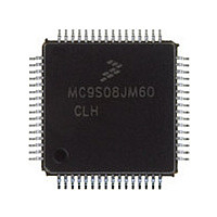
MC9S08JM60CLH Freescale, MC9S08JM60CLH Datasheet - Page 196

MC9S08JM60CLH
Manufacturer Part Number
MC9S08JM60CLH
Description
Manufacturer
Freescale
Datasheet
1.MC9S08JM60CLH.pdf
(388 pages)
Specifications of MC9S08JM60CLH
Cpu Family
HCS08
Device Core Size
8b
Frequency (max)
24MHz
Interface Type
SCI/SPI
Total Internal Ram Size
4KB
# I/os (max)
51
Number Of Timers - General Purpose
8
Operating Supply Voltage (typ)
3.3/5V
Operating Supply Voltage (max)
5.5V
Operating Supply Voltage (min)
2.7V
On-chip Adc
12-chx12-bit
Instruction Set Architecture
CISC
Operating Temp Range
-40C to 85C
Operating Temperature Classification
Industrial
Mounting
Surface Mount
Pin Count
64
Package Type
LQFP
Program Memory Type
Flash
Program Memory Size
60KB
Lead Free Status / RoHS Status
Compliant
Available stocks
Company
Part Number
Manufacturer
Quantity
Price
Company:
Part Number:
MC9S08JM60CLH
Manufacturer:
Freescale Semiconductor
Quantity:
10 000
Part Number:
MC9S08JM60CLH
Manufacturer:
FREESCALE
Quantity:
20 000
Company:
Part Number:
MC9S08JM60CLHE
Manufacturer:
AZBIL
Quantity:
1 000
- Current page: 196 of 388
- Download datasheet (5Mb)
Multi-Purpose Clock Generator (S08MCGV1)
In bypassed low power external mode, the MCGOUT clock is derived from the external reference clock.
The external reference clock which is enabled can be an external crystal/resonator or it can be another
external clock source.
The PLL and the FLL are disabled at all times in BLPE mode and the MCGLCLK will not be available
for BDC communications. If the BDM becomes active the mode will switch to one of the bypassed
external modes as determined by the state of the PLLS bit.
12.4.1.9
Stop mode is entered whenever the MCU enters a STOP state. In this mode, the FLL and PLL are disabled
and all MCG clock signals are static except in the following cases:
MCGIRCLK will be active in stop mode when all the following conditions occur:
MCGERCLK will be active in stop mode when all the following conditions occur:
12.4.2
When switching between engaged internal and engaged external modes the IREFS bit can be changed at
anytime, but the RDIV bits must be changed simultaneously so that the reference frequency stays in the
range required by the state of the PLLS bit (31.25 kHz to 39.0625 kHz if the FLL is selected, or 1 MHz to
2 MHz if the PLL is selected). After a change in the IREFS value the FLL or PLL will begin locking again
after the switch is completed. The completion of the switch is shown by the IREFST bit.
For the special case of entering stop mode immediately after switching to FBE mode, if the external clock
and the internal clock are disabled in stop mode, (EREFSTEN = 0 and IREFSTEN = 0), it is necessary to
allow 100us after the IREFST bit is cleared to allow the internal reference to shutdown. For most cases the
delay due to instruction execution times will be sufficient.
The CLKS bits can also be changed at anytime, but in order for the MCGLCLK to be configured correctly
the RDIV bits must be changed simultaneously so that the reference frequency stays in the range required
by the state of the PLLS bit (31.25 kHz to 39.0625 kHz if the FLL is selected, or 1 MHz to 2MHz if the
PLL is selected). The actual switch to the newly selected clock will be shown by the CLKST bits. If the
newly selected clock is not available, the previous clock will remain selected.
For details see
12.4.3
The BDIV bits can be changed at anytime and the actual switch to the new frequency will occur
immediately.
196
•
•
•
•
IRCLKEN = 1
IREFSTEN = 1
ERCLKEN = 1
EREFSTEN = 1
Mode Switching
Bus Frequency Divider
Stop
Figure
12-8.
MC9S08JM60 Series Data Sheet, Rev. 3
Freescale Semiconductor
Related parts for MC9S08JM60CLH
Image
Part Number
Description
Manufacturer
Datasheet
Request
R

Part Number:
Description:
TOWER ELEVATOR BOARDS HARDWARE
Manufacturer:
Freescale Semiconductor
Datasheet:

Part Number:
Description:
TOWER SERIAL I/O HARDWARE
Manufacturer:
Freescale Semiconductor
Datasheet:

Part Number:
Description:
LCD MODULE FOR TWR SYSTEM
Manufacturer:
Freescale Semiconductor
Datasheet:

Part Number:
Description:
DAUGHTER LCD WVGA I.MX51
Manufacturer:
Freescale Semiconductor
Datasheet:

Part Number:
Description:
TOWER SYSTEM BOARD MPC5125
Manufacturer:
Freescale Semiconductor
Datasheet:

Part Number:
Description:
KIT EVALUATION I.MX51
Manufacturer:
Freescale Semiconductor
Datasheet:

Part Number:
Description:
KIT DEVELOPMENT WINCE IMX25
Manufacturer:
Freescale Semiconductor
Datasheet:

Part Number:
Description:
TOWER SYSTEM KIT MPC5125
Manufacturer:
Freescale Semiconductor
Datasheet:

Part Number:
Description:
TOWER SYSTEM BOARD K40X256
Manufacturer:
Freescale Semiconductor
Datasheet:

Part Number:
Description:
TOWER SYSTEM KIT K40X256
Manufacturer:
Freescale Semiconductor
Datasheet:

Part Number:
Description:
Microcontrollers (MCU) MX28 PLATFORM DEV KIT
Manufacturer:
Freescale Semiconductor
Datasheet:

Part Number:
Description:
MCU, MPU & DSP Development Tools IAR KickStart Kit for Kinetis K60
Manufacturer:
Freescale Semiconductor
Datasheet:

Part Number:
Description:
24BIT HDMI MX535/08
Manufacturer:
Freescale Semiconductor
Datasheet:
Part Number:
Description:
Manufacturer:
Freescale Semiconductor, Inc
Datasheet:
Part Number:
Description:
Manufacturer:
Freescale Semiconductor, Inc
Datasheet:


