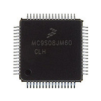
MC9S08JM60CLH Freescale, MC9S08JM60CLH Datasheet - Page 337

MC9S08JM60CLH
Manufacturer Part Number
MC9S08JM60CLH
Description
Manufacturer
Freescale
Datasheet
1.MC9S08JM60CLH.pdf
(388 pages)
Specifications of MC9S08JM60CLH
Cpu Family
HCS08
Device Core Size
8b
Frequency (max)
24MHz
Interface Type
SCI/SPI
Total Internal Ram Size
4KB
# I/os (max)
51
Number Of Timers - General Purpose
8
Operating Supply Voltage (typ)
3.3/5V
Operating Supply Voltage (max)
5.5V
Operating Supply Voltage (min)
2.7V
On-chip Adc
12-chx12-bit
Instruction Set Architecture
CISC
Operating Temp Range
-40C to 85C
Operating Temperature Classification
Industrial
Mounting
Surface Mount
Pin Count
64
Package Type
LQFP
Program Memory Type
Flash
Program Memory Size
60KB
Lead Free Status / RoHS Status
Compliant
Available stocks
Company
Part Number
Manufacturer
Quantity
Price
Company:
Part Number:
MC9S08JM60CLH
Manufacturer:
Freescale Semiconductor
Quantity:
10 000
Part Number:
MC9S08JM60CLH
Manufacturer:
FREESCALE
Quantity:
20 000
Company:
Part Number:
MC9S08JM60CLHE
Manufacturer:
AZBIL
Quantity:
1 000
- Current page: 337 of 388
- Download datasheet (5Mb)
18.3
Because HCS08 devices do not have external address and data buses, the most important functions of an
in-circuit emulator have been built onto the chip with the MCU. The debug system consists of an 8-stage
FIFO that can store address or data bus information, and a flexible trigger system to decide when to capture
bus information and what information to capture. The system relies on the single-wire background debug
system to access debug control registers and to read results out of the eight stage FIFO.
The debug module includes control and status registers that are accessible in the user’s memory map.
These registers are located in the high register space to avoid using valuable direct page memory space.
Most of the debug module’s functions are used during development, and user programs rarely access any
of the control and status registers for the debug module. The one exception is that the debug system can
provide the means to implement a form of ROM patching. This topic is discussed in greater detail in
Section 18.3.6, “Hardware
18.3.1
Two 16-bit comparators (A and B) can optionally be qualified with the R/W signal and an opcode tracking
circuit. Separate control bits allow you to ignore R/W for each comparator. The opcode tracking circuitry
optionally allows you to specify that a trigger will occur only if the opcode at the specified address is
actually executed as opposed to only being read from memory into the instruction queue. The comparators
are also capable of magnitude comparisons to support the inside range and outside range trigger modes.
Comparators are disabled temporarily during all BDC accesses.
The A comparator is always associated with the 16-bit CPU address. The B comparator compares to the
CPU address or the 8-bit CPU data bus, depending on the trigger mode selected. Because the CPU data
bus is separated into a read data bus and a write data bus, the RWAEN and RWA control bits have an
additional purpose, in full address plus data comparisons they are used to decide which of these buses to
use in the comparator B data bus comparisons. If RWAEN = 1 (enabled) and RWA = 0 (write), the CPU’s
write data bus is used. Otherwise, the CPU’s read data bus is used.
The currently selected trigger mode determines what the debugger logic does when a comparator detects
a qualified match condition. A match can cause:
18.3.2
The usual way to use the FIFO is to setup the trigger mode and other control options, then arm the
debugger. When the FIFO has filled or the debugger has stopped storing data into the FIFO, you would
read the information out of it in the order it was stored into the FIFO. Status bits indicate the number of
words of valid information that are in the FIFO as data is stored into it. If a trace run is manually halted by
writing 0 to ARM before the FIFO is full (CNT = 1:0:0:0), the information is shifted by one position and
Freescale Semiconductor
•
•
•
•
Generation of a breakpoint to the CPU
Storage of data bus values into the FIFO
Starting to store change-of-flow addresses into the FIFO (begin type trace)
Stopping the storage of change-of-flow addresses into the FIFO (end type trace)
On-Chip Debug System (DBG)
Comparators A and B
Bus Capture Information and FIFO Operation
Breakpoints.”
MC9S08JM60 Series Data Sheet, Rev. 3
Development Support
337
Related parts for MC9S08JM60CLH
Image
Part Number
Description
Manufacturer
Datasheet
Request
R

Part Number:
Description:
TOWER ELEVATOR BOARDS HARDWARE
Manufacturer:
Freescale Semiconductor
Datasheet:

Part Number:
Description:
TOWER SERIAL I/O HARDWARE
Manufacturer:
Freescale Semiconductor
Datasheet:

Part Number:
Description:
LCD MODULE FOR TWR SYSTEM
Manufacturer:
Freescale Semiconductor
Datasheet:

Part Number:
Description:
DAUGHTER LCD WVGA I.MX51
Manufacturer:
Freescale Semiconductor
Datasheet:

Part Number:
Description:
TOWER SYSTEM BOARD MPC5125
Manufacturer:
Freescale Semiconductor
Datasheet:

Part Number:
Description:
KIT EVALUATION I.MX51
Manufacturer:
Freescale Semiconductor
Datasheet:

Part Number:
Description:
KIT DEVELOPMENT WINCE IMX25
Manufacturer:
Freescale Semiconductor
Datasheet:

Part Number:
Description:
TOWER SYSTEM KIT MPC5125
Manufacturer:
Freescale Semiconductor
Datasheet:

Part Number:
Description:
TOWER SYSTEM BOARD K40X256
Manufacturer:
Freescale Semiconductor
Datasheet:

Part Number:
Description:
TOWER SYSTEM KIT K40X256
Manufacturer:
Freescale Semiconductor
Datasheet:

Part Number:
Description:
Microcontrollers (MCU) MX28 PLATFORM DEV KIT
Manufacturer:
Freescale Semiconductor
Datasheet:

Part Number:
Description:
MCU, MPU & DSP Development Tools IAR KickStart Kit for Kinetis K60
Manufacturer:
Freescale Semiconductor
Datasheet:

Part Number:
Description:
24BIT HDMI MX535/08
Manufacturer:
Freescale Semiconductor
Datasheet:
Part Number:
Description:
Manufacturer:
Freescale Semiconductor, Inc
Datasheet:
Part Number:
Description:
Manufacturer:
Freescale Semiconductor, Inc
Datasheet:


