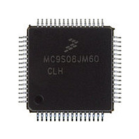
MC9S08JM60CLH Freescale, MC9S08JM60CLH Datasheet - Page 68

MC9S08JM60CLH
Manufacturer Part Number
MC9S08JM60CLH
Description
Manufacturer
Freescale
Datasheet
1.MC9S08JM60CLH.pdf
(388 pages)
Specifications of MC9S08JM60CLH
Cpu Family
HCS08
Device Core Size
8b
Frequency (max)
24MHz
Interface Type
SCI/SPI
Total Internal Ram Size
4KB
# I/os (max)
51
Number Of Timers - General Purpose
8
Operating Supply Voltage (typ)
3.3/5V
Operating Supply Voltage (max)
5.5V
Operating Supply Voltage (min)
2.7V
On-chip Adc
12-chx12-bit
Instruction Set Architecture
CISC
Operating Temp Range
-40C to 85C
Operating Temperature Classification
Industrial
Mounting
Surface Mount
Pin Count
64
Package Type
LQFP
Program Memory Type
Flash
Program Memory Size
60KB
Lead Free Status / RoHS Status
Compliant
Available stocks
Company
Part Number
Manufacturer
Quantity
Price
Company:
Part Number:
MC9S08JM60CLH
Manufacturer:
Freescale Semiconductor
Quantity:
10 000
Part Number:
MC9S08JM60CLH
Manufacturer:
FREESCALE
Quantity:
20 000
Company:
Part Number:
MC9S08JM60CLHE
Manufacturer:
AZBIL
Quantity:
1 000
- Current page: 68 of 388
- Download datasheet (5Mb)
Chapter 5 Resets, Interrupts, and System Configuration
5.5.1
Figure 5-1
(SP) points at the next available byte location on the stack. The current values of CPU registers are stored
on the stack starting with the low-order byte of the program counter (PCL) and ending with the CCR. After
stacking, the SP points at the next available location on the stack which is the address that is one less than
the address where the CCR was saved. The PC value that is stacked is the address of the instruction in the
main program that would have executed next if the interrupt had not occurred.
When an RTI instruction is executed, these values are recovered from the stack in reverse order. As part
of the RTI sequence, the CPU fills the instruction pipeline by reading three bytes of program information,
starting from the PC address recovered from the stack.
The status flag causing the interrupt must be acknowledged (cleared) before returning from the ISR.
Typically, the flag must be cleared at the beginning of the ISR so that if another interrupt is generated by
this same source, it will be registered so it can be serviced after completion of the current ISR.
5.5.2
External interrupts are managed by the IRQSC status and control register. When the IRQ function is
enabled, synchronous logic monitors the pin for edge-only or edge-and-level events. When the MCU is in
stop mode and system clocks are shut down, a separate asynchronous path is used so the IRQ (if enabled)
can wake the MCU.
5.5.2.1
The IRQ pin enable (IRQPE) control bit in IRQSC must be 1 in order for the IRQ pin to act as the interrupt
request (IRQ) input. As an IRQ input, the user can choose the polarity of edges or levels detected
(IRQEDG), whether the pin detects edges-only or edges and levels (IRQMOD), and whether an event
causes an interrupt or only sets the IRQF flag which can be polled by software.
68
shows the contents and organization of a stack frame. Before the interrupt, the stack pointer
Interrupt Stack Frame
External Interrupt Request (IRQ) Pin
Pin Configuration Options
STACKING
ORDER
UNSTACKING
5
4
3
2
1
ORDER
1
2
3
4
5
* High byte (H) of index register is not automatically stacked.
7
INDEX REGISTER (LOW BYTE X)
MC9S08JM60 Series Data Sheet, Rev. 3
Figure 5-1. Interrupt Stack Frame
CONDITION CODE REGISTER
PROGRAM COUNTER HIGH
PROGRAM COUNTER LOW
ACCUMULATOR
TOWARD HIGHER ADDRESSES
TOWARD LOWER ADDRESSES
*
0
SP AFTER
INTERRUPT STACKING
SP BEFORE
THE INTERRUPT
Freescale Semiconductor
Related parts for MC9S08JM60CLH
Image
Part Number
Description
Manufacturer
Datasheet
Request
R

Part Number:
Description:
TOWER ELEVATOR BOARDS HARDWARE
Manufacturer:
Freescale Semiconductor
Datasheet:

Part Number:
Description:
TOWER SERIAL I/O HARDWARE
Manufacturer:
Freescale Semiconductor
Datasheet:

Part Number:
Description:
LCD MODULE FOR TWR SYSTEM
Manufacturer:
Freescale Semiconductor
Datasheet:

Part Number:
Description:
DAUGHTER LCD WVGA I.MX51
Manufacturer:
Freescale Semiconductor
Datasheet:

Part Number:
Description:
TOWER SYSTEM BOARD MPC5125
Manufacturer:
Freescale Semiconductor
Datasheet:

Part Number:
Description:
KIT EVALUATION I.MX51
Manufacturer:
Freescale Semiconductor
Datasheet:

Part Number:
Description:
KIT DEVELOPMENT WINCE IMX25
Manufacturer:
Freescale Semiconductor
Datasheet:

Part Number:
Description:
TOWER SYSTEM KIT MPC5125
Manufacturer:
Freescale Semiconductor
Datasheet:

Part Number:
Description:
TOWER SYSTEM BOARD K40X256
Manufacturer:
Freescale Semiconductor
Datasheet:

Part Number:
Description:
TOWER SYSTEM KIT K40X256
Manufacturer:
Freescale Semiconductor
Datasheet:

Part Number:
Description:
Microcontrollers (MCU) MX28 PLATFORM DEV KIT
Manufacturer:
Freescale Semiconductor
Datasheet:

Part Number:
Description:
MCU, MPU & DSP Development Tools IAR KickStart Kit for Kinetis K60
Manufacturer:
Freescale Semiconductor
Datasheet:

Part Number:
Description:
24BIT HDMI MX535/08
Manufacturer:
Freescale Semiconductor
Datasheet:
Part Number:
Description:
Manufacturer:
Freescale Semiconductor, Inc
Datasheet:
Part Number:
Description:
Manufacturer:
Freescale Semiconductor, Inc
Datasheet:


