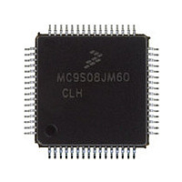
MC9S08JM60CLH Freescale, MC9S08JM60CLH Datasheet - Page 29

MC9S08JM60CLH
Manufacturer Part Number
MC9S08JM60CLH
Description
Manufacturer
Freescale
Datasheet
1.MC9S08JM60CLH.pdf
(388 pages)
Specifications of MC9S08JM60CLH
Cpu Family
HCS08
Device Core Size
8b
Frequency (max)
24MHz
Interface Type
SCI/SPI
Total Internal Ram Size
4KB
# I/os (max)
51
Number Of Timers - General Purpose
8
Operating Supply Voltage (typ)
3.3/5V
Operating Supply Voltage (max)
5.5V
Operating Supply Voltage (min)
2.7V
On-chip Adc
12-chx12-bit
Instruction Set Architecture
CISC
Operating Temp Range
-40C to 85C
Operating Temperature Classification
Industrial
Mounting
Surface Mount
Pin Count
64
Package Type
LQFP
Program Memory Type
Flash
Program Memory Size
60KB
Lead Free Status / RoHS Status
Compliant
Available stocks
Company
Part Number
Manufacturer
Quantity
Price
Company:
Part Number:
MC9S08JM60CLH
Manufacturer:
Freescale Semiconductor
Quantity:
10 000
Part Number:
MC9S08JM60CLH
Manufacturer:
FREESCALE
Quantity:
20 000
Company:
Part Number:
MC9S08JM60CLHE
Manufacturer:
AZBIL
Quantity:
1 000
- Current page: 29 of 388
- Download datasheet (5Mb)
Freescale Semiconductor
NOTES:
1. External crystal circuity is not required if using the MCG internal clock option. For USB operation, an external crystal is required.
2. XTAL and EXTAL are the same pins as PTG4 and PTG5, respectively.
3. RC filters on RESET and IRQ are recommended for EMC-sensitive applications.
4. R
5. V
6. USBDP and USBDN are powered by the 3.3-V regulator or external 3.3-V supply on V
V
The voltage regulator output is used for R
DD
PUDP
BUS
SYSTEM
POWER
NOTE 1
BACKGROUND HEADER
OPTIONAL
is a 5.0-V supply from upstream port that can be used for USB operation
MANUAL
RESET
is shown for full-speed USB only. The diagram shows a configuration where the on-chip regulator and R
C1
USB SERIES-B CONNECTOR
5 V
+
ASYNCHRONOUS
10 μF
INTERRUPT
C
X1
INPUT
BLK
3.3-V Reference
4.7 μF
V
+
R
DD
F
2
3
+
1
4
V
C2
DD
4.7 kΩ–10 kΩ
0.1 μF
C
Figure 2-4. Basic System Connections
0.1 μF
BY
V
MC9S08JM60 Series Data Sheet, Rev. 3
Bus
C
0.1 μF
BYAD
R
PUDP.
S
V
0.47 μF
DD
4.7 kΩ–
10 kΩ
0.1 μF
R
PUDP
V
USBDN
V
can optionally be disabled if using an external pullup resistor on USBDP
V
USB33
V
V
V
V
V
XTAL
USB33
EXTAL
V
REFL
REFH
DDAD
DD
SSAD
SS
SSOSC
R
BKGD/MS
PUDP
RESET
IRQ
USBDP
MC9S08JM60
PORT
PORT
PORT
PORT
PORT
PORT
PORT
B
C
D
E
G
A
F
USB33
.
Chapter 2 Pins and Connections
PTA0–PTA5
PTB0/MISO2/ADP0
PTB1/MOSI2/ADP1
PTB2/SPSCK2/ADP2
PTB3/SS2/ADP3
PTB4/KBIP4/ADP4
PTB5/KBIP5/ADP5
PTB6/ADP6
PTB7/ADP7
PTC0/SCL
PTC1/SDA
PTC2
PTC3/TxD2
PTC4
PTC5/RxD2
PTC6
PTD0/ADP8/ACMP+
PTD1/ADP9/ACMP–
PTD2/KBIP2/ACMPO
PTD3/KBIP3/ADP10
PTD4/ADP11
PTD5
PTD6
PTD7
PTE0/TxD1
PTE1/RxD1
PTE2/TPM1CH0
PTE3/TPM1CH1
PTE4/MISO1
PTE5/MOSI1
PTE6/SPSCK1
PTE7/SS1
PTF0/TPM1CH2
PTF1/TPM1CH3
PTF2/TPM1CH4
PTF3/TPM1CH5
PTF4/TPM2CH0
PTF5/TPM2CH1
PTF6
PTF7
PTG0/KBIP0
PTG1/KBIP1
PTG2/KBIP6
PTG3/KBIP7
PTG4/XTAL
PTG5/EXTAL
PUDP
are enabled.
INTERFACE TO
APPLICATION
PERIPHERAL
SYSTEM
I/O AND
29
Related parts for MC9S08JM60CLH
Image
Part Number
Description
Manufacturer
Datasheet
Request
R

Part Number:
Description:
TOWER ELEVATOR BOARDS HARDWARE
Manufacturer:
Freescale Semiconductor
Datasheet:

Part Number:
Description:
TOWER SERIAL I/O HARDWARE
Manufacturer:
Freescale Semiconductor
Datasheet:

Part Number:
Description:
LCD MODULE FOR TWR SYSTEM
Manufacturer:
Freescale Semiconductor
Datasheet:

Part Number:
Description:
DAUGHTER LCD WVGA I.MX51
Manufacturer:
Freescale Semiconductor
Datasheet:

Part Number:
Description:
TOWER SYSTEM BOARD MPC5125
Manufacturer:
Freescale Semiconductor
Datasheet:

Part Number:
Description:
KIT EVALUATION I.MX51
Manufacturer:
Freescale Semiconductor
Datasheet:

Part Number:
Description:
KIT DEVELOPMENT WINCE IMX25
Manufacturer:
Freescale Semiconductor
Datasheet:

Part Number:
Description:
TOWER SYSTEM KIT MPC5125
Manufacturer:
Freescale Semiconductor
Datasheet:

Part Number:
Description:
TOWER SYSTEM BOARD K40X256
Manufacturer:
Freescale Semiconductor
Datasheet:

Part Number:
Description:
TOWER SYSTEM KIT K40X256
Manufacturer:
Freescale Semiconductor
Datasheet:

Part Number:
Description:
Microcontrollers (MCU) MX28 PLATFORM DEV KIT
Manufacturer:
Freescale Semiconductor
Datasheet:

Part Number:
Description:
MCU, MPU & DSP Development Tools IAR KickStart Kit for Kinetis K60
Manufacturer:
Freescale Semiconductor
Datasheet:

Part Number:
Description:
24BIT HDMI MX535/08
Manufacturer:
Freescale Semiconductor
Datasheet:
Part Number:
Description:
Manufacturer:
Freescale Semiconductor, Inc
Datasheet:
Part Number:
Description:
Manufacturer:
Freescale Semiconductor, Inc
Datasheet:


