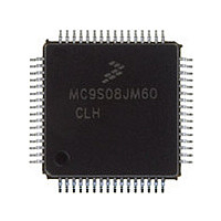
MC9S08JM60CLH Freescale, MC9S08JM60CLH Datasheet - Page 350

MC9S08JM60CLH
Manufacturer Part Number
MC9S08JM60CLH
Description
Manufacturer
Freescale
Datasheet
1.MC9S08JM60CLH.pdf
(388 pages)
Specifications of MC9S08JM60CLH
Cpu Family
HCS08
Device Core Size
8b
Frequency (max)
24MHz
Interface Type
SCI/SPI
Total Internal Ram Size
4KB
# I/os (max)
51
Number Of Timers - General Purpose
8
Operating Supply Voltage (typ)
3.3/5V
Operating Supply Voltage (max)
5.5V
Operating Supply Voltage (min)
2.7V
On-chip Adc
12-chx12-bit
Instruction Set Architecture
CISC
Operating Temp Range
-40C to 85C
Operating Temperature Classification
Industrial
Mounting
Surface Mount
Pin Count
64
Package Type
LQFP
Program Memory Type
Flash
Program Memory Size
60KB
Lead Free Status / RoHS Status
Compliant
Available stocks
Company
Part Number
Manufacturer
Quantity
Price
Company:
Part Number:
MC9S08JM60CLH
Manufacturer:
Freescale Semiconductor
Quantity:
10 000
Part Number:
MC9S08JM60CLH
Manufacturer:
FREESCALE
Quantity:
20 000
Company:
Part Number:
MC9S08JM60CLHE
Manufacturer:
AZBIL
Quantity:
1 000
- Current page: 350 of 388
- Download datasheet (5Mb)
Appendix A Electrical Characteristics
A.4
This section provides information about operating temperature range, power dissipation, and package
thermal resistance. Power dissipation on I/O pins is usually small compared to the power dissipation in
on-chip logic and it is user-determined rather than being controlled by the MCU design. In order to take
P
V
loads), the difference between pin voltage and V
350
I/O
DD
into account in power calculations, determine the difference between actual pin voltage and V
Num
and multiply by the pin current for each I/O pin. Except in cases of unusually high pin current (heavy
1
2
3
Thermal Characteristics
C
T Operating temperature range (packaged)
D Maximum junction temperature
T
1
2
3
Supply voltage
Input voltage
Instantaneous maximum current
Maximum current into V
Storage temperature
Input must be current limited to the value specified. To determine the value of the required
current-limiting resistor, calculate resistance values for positive (V
voltages, then use the larger of the two resistance values.
All functional non-supply pins are internally clamped to V
Power supply must maintain regulation within operating V
operating maximum current conditions. If positive injection current (V
I
out of regulation. Ensure external V
current. This will be the greatest risk when the MCU is not consuming power. Examples are: if
no system clock is present, or if the clock rate is very low which would reduce overall power
consumption.
Single pin limit (applies to all port pins)
Thermal resistance
DD
Single layer board
Four layer board
, the injection current may flow out of V
Rating
Rating
DD
Table A-2. Absolute Maximum Ratings
MC9S08JM60 Series Data Sheet, Rev. 3
Table A-3. Thermal Characteristics
64-pin LQFP
44-pin LQFP
64-pin LQFP
44-pin LQFP
DD
48-pin QFN
48-pin QFN
64-pin QFP
64-pin QFP
load will shunt current greater than maximum injection
1
,
2
SS
DD
,
3
or V
and could result in external power supply going
DD
Symbol
Symbol
θ
will be very small.
T
T
T
V
JA
A
V
I
J
I
DD
stg
DD
SS
D
In
DD
and V
range during instantaneous and
DD
– 0.3 to V
DD
) and negative (V
– 0.3 to + 5.8
.
–55 to +150
In
–40 to 85
> V
Value
Value
135
± 25
55
73
84
71
41
54
28
49
120
DD
DD
) is greater than
+ 0.3
Freescale Semiconductor
SS
) clamp
°C/W
Unit
Unit
mA
mA
°C
°C
°C
V
V
Temp.
Code
—
C
SS
or
Related parts for MC9S08JM60CLH
Image
Part Number
Description
Manufacturer
Datasheet
Request
R

Part Number:
Description:
TOWER ELEVATOR BOARDS HARDWARE
Manufacturer:
Freescale Semiconductor
Datasheet:

Part Number:
Description:
TOWER SERIAL I/O HARDWARE
Manufacturer:
Freescale Semiconductor
Datasheet:

Part Number:
Description:
LCD MODULE FOR TWR SYSTEM
Manufacturer:
Freescale Semiconductor
Datasheet:

Part Number:
Description:
DAUGHTER LCD WVGA I.MX51
Manufacturer:
Freescale Semiconductor
Datasheet:

Part Number:
Description:
TOWER SYSTEM BOARD MPC5125
Manufacturer:
Freescale Semiconductor
Datasheet:

Part Number:
Description:
KIT EVALUATION I.MX51
Manufacturer:
Freescale Semiconductor
Datasheet:

Part Number:
Description:
KIT DEVELOPMENT WINCE IMX25
Manufacturer:
Freescale Semiconductor
Datasheet:

Part Number:
Description:
TOWER SYSTEM KIT MPC5125
Manufacturer:
Freescale Semiconductor
Datasheet:

Part Number:
Description:
TOWER SYSTEM BOARD K40X256
Manufacturer:
Freescale Semiconductor
Datasheet:

Part Number:
Description:
TOWER SYSTEM KIT K40X256
Manufacturer:
Freescale Semiconductor
Datasheet:

Part Number:
Description:
Microcontrollers (MCU) MX28 PLATFORM DEV KIT
Manufacturer:
Freescale Semiconductor
Datasheet:

Part Number:
Description:
MCU, MPU & DSP Development Tools IAR KickStart Kit for Kinetis K60
Manufacturer:
Freescale Semiconductor
Datasheet:

Part Number:
Description:
24BIT HDMI MX535/08
Manufacturer:
Freescale Semiconductor
Datasheet:
Part Number:
Description:
Manufacturer:
Freescale Semiconductor, Inc
Datasheet:
Part Number:
Description:
Manufacturer:
Freescale Semiconductor, Inc
Datasheet:


