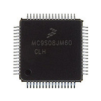
MC9S08JM60CLH Freescale, MC9S08JM60CLH Datasheet - Page 71

MC9S08JM60CLH
Manufacturer Part Number
MC9S08JM60CLH
Description
Manufacturer
Freescale
Datasheet
1.MC9S08JM60CLH.pdf
(388 pages)
Specifications of MC9S08JM60CLH
Cpu Family
HCS08
Device Core Size
8b
Frequency (max)
24MHz
Interface Type
SCI/SPI
Total Internal Ram Size
4KB
# I/os (max)
51
Number Of Timers - General Purpose
8
Operating Supply Voltage (typ)
3.3/5V
Operating Supply Voltage (max)
5.5V
Operating Supply Voltage (min)
2.7V
On-chip Adc
12-chx12-bit
Instruction Set Architecture
CISC
Operating Temp Range
-40C to 85C
Operating Temperature Classification
Industrial
Mounting
Surface Mount
Pin Count
64
Package Type
LQFP
Program Memory Type
Flash
Program Memory Size
60KB
Lead Free Status / RoHS Status
Compliant
Available stocks
Company
Part Number
Manufacturer
Quantity
Price
Company:
Part Number:
MC9S08JM60CLH
Manufacturer:
Freescale Semiconductor
Quantity:
10 000
Part Number:
MC9S08JM60CLH
Manufacturer:
FREESCALE
Quantity:
20 000
Company:
Part Number:
MC9S08JM60CLHE
Manufacturer:
AZBIL
Quantity:
1 000
- Current page: 71 of 388
- Download datasheet (5Mb)
5.6
The MC9S08JM60 series includes a system to protect against low-voltage conditions in order to protect
memory contents and control MCU system states during supply voltage variations. The system is
comprised of a power-on reset (POR) circuit and a LVD circuit with trip voltages for warning and
detection. The LVD circuit is enabled when LVDE in SPMSC1 is set to 1. The LVD is disabled upon
entering any of the stop modes unless LVDSE is set in SPMSC1. If LVDSE and LVDE are both set, then
the MCU cannot enter stop2 (it will enter stop3 instead), and the current consumption in stop3 with the
LVD enabled will be higher.
5.6.1
When power is initially applied to the MCU, or when the supply voltage drops below the power-on reset
rearm voltage level, V
LVD circuit will hold the MCU in reset until the supply has risen above the low voltage detection low
threshold, V
5.6.2
The LVD can be configured to generate a reset upon detection of a low voltage condition by setting
LVDRE to 1. The low voltage detection threshold is determined by the LVDV bit. After an LVD reset has
occurred, the LVD system will hold the MCU in reset until the supply voltage has risen above the low
voltage detection threshold. The LVD bit in the SRS register is set following either an LVD reset or POR.
5.6.3
The LVD system has a low voltage warning flag to indicate to the user that the supply voltage is
approaching the low voltage condition. When a low voltage warning condition is detected and is
configured for interrupt operation (LVWIE set to 1), LVWF in SPMSC1 will be set and an LVW interrupt
request will occur.
Freescale Semiconductor
Number
Vector
1
0
Low-Voltage Detect (LVD) System
Power-On Reset Operation
Low-Voltage Detection (LVD) Reset Operation
Low-Voltage Warning (LVW) Interrupt Operation
LVDL
0xFFFC:FFFD
0xFFFE:FFFF
(High/Low)
Address
Table 5-1. Vector Summary (from Lowest to Highest Priority) (continued)
. Both the POR bit and the LVD bit in SRS are set following a POR.
POR
, the POR circuit will cause a reset condition. As the supply voltage rises, the
Vector Name
Vreset
Vswi
MC9S08JM60 Series Data Sheet, Rev. 3
Module
System
control
Core
SWI Instruction
Illegal opcode
RESET pin
Source
BDFR
COP
POR
LOC
LVD
Chapter 5 Resets, Interrupts, and System Configuration
Enable
LVDRE
COPE
BDFR
ILOP
CME
POR
—
—
Low-voltage detect
Software interrupt
BDM-forced reset
Watchdog timer
Power-on-reset
Illegal opcode
Loss of clock
Description
External pin
71
Related parts for MC9S08JM60CLH
Image
Part Number
Description
Manufacturer
Datasheet
Request
R

Part Number:
Description:
TOWER ELEVATOR BOARDS HARDWARE
Manufacturer:
Freescale Semiconductor
Datasheet:

Part Number:
Description:
TOWER SERIAL I/O HARDWARE
Manufacturer:
Freescale Semiconductor
Datasheet:

Part Number:
Description:
LCD MODULE FOR TWR SYSTEM
Manufacturer:
Freescale Semiconductor
Datasheet:

Part Number:
Description:
DAUGHTER LCD WVGA I.MX51
Manufacturer:
Freescale Semiconductor
Datasheet:

Part Number:
Description:
TOWER SYSTEM BOARD MPC5125
Manufacturer:
Freescale Semiconductor
Datasheet:

Part Number:
Description:
KIT EVALUATION I.MX51
Manufacturer:
Freescale Semiconductor
Datasheet:

Part Number:
Description:
KIT DEVELOPMENT WINCE IMX25
Manufacturer:
Freescale Semiconductor
Datasheet:

Part Number:
Description:
TOWER SYSTEM KIT MPC5125
Manufacturer:
Freescale Semiconductor
Datasheet:

Part Number:
Description:
TOWER SYSTEM BOARD K40X256
Manufacturer:
Freescale Semiconductor
Datasheet:

Part Number:
Description:
TOWER SYSTEM KIT K40X256
Manufacturer:
Freescale Semiconductor
Datasheet:

Part Number:
Description:
Microcontrollers (MCU) MX28 PLATFORM DEV KIT
Manufacturer:
Freescale Semiconductor
Datasheet:

Part Number:
Description:
MCU, MPU & DSP Development Tools IAR KickStart Kit for Kinetis K60
Manufacturer:
Freescale Semiconductor
Datasheet:

Part Number:
Description:
24BIT HDMI MX535/08
Manufacturer:
Freescale Semiconductor
Datasheet:
Part Number:
Description:
Manufacturer:
Freescale Semiconductor, Inc
Datasheet:
Part Number:
Description:
Manufacturer:
Freescale Semiconductor, Inc
Datasheet:


