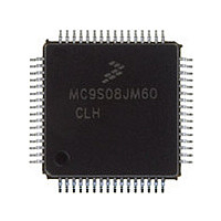
MC9S08JM60CLH Freescale, MC9S08JM60CLH Datasheet - Page 246

MC9S08JM60CLH
Manufacturer Part Number
MC9S08JM60CLH
Description
Manufacturer
Freescale
Datasheet
1.MC9S08JM60CLH.pdf
(388 pages)
Specifications of MC9S08JM60CLH
Cpu Family
HCS08
Device Core Size
8b
Frequency (max)
24MHz
Interface Type
SCI/SPI
Total Internal Ram Size
4KB
# I/os (max)
51
Number Of Timers - General Purpose
8
Operating Supply Voltage (typ)
3.3/5V
Operating Supply Voltage (max)
5.5V
Operating Supply Voltage (min)
2.7V
On-chip Adc
12-chx12-bit
Instruction Set Architecture
CISC
Operating Temp Range
-40C to 85C
Operating Temperature Classification
Industrial
Mounting
Surface Mount
Pin Count
64
Package Type
LQFP
Program Memory Type
Flash
Program Memory Size
60KB
Lead Free Status / RoHS Status
Compliant
Available stocks
Company
Part Number
Manufacturer
Quantity
Price
Company:
Part Number:
MC9S08JM60CLH
Manufacturer:
Freescale Semiconductor
Quantity:
10 000
Part Number:
MC9S08JM60CLH
Manufacturer:
FREESCALE
Quantity:
20 000
Company:
Part Number:
MC9S08JM60CLHE
Manufacturer:
AZBIL
Quantity:
1 000
- Current page: 246 of 388
- Download datasheet (5Mb)
Serial Peripheral Interface (S08SPI16V1)
15.1.2
The SPI includes these distinctive features:
15.1.3
The SPI functions in three modes, run, wait, and stop.
The SPI is completely disabled in all other stop modes. When the CPU wakes from these stop modes, all
SPI register content will be reset.
This is a high level description only, detailed descriptions of operating modes are contained in section
Section 15.4.9, “Low Power Mode
15.1.4
This section includes block diagrams showing SPI system connections, the internal organization of the SPI
module, and the SPI clock dividers that control the master mode bit rate.
246
•
•
•
•
•
•
•
•
•
•
•
•
•
•
Master mode or slave mode operation
Full-duplex or single-wire bidirectional mode
Programmable transmit bit rate
Double-buffered transmit and receive data register
Serial clock phase and polarity options
Slave select output
Mode fault error flag with CPU interrupt capability
Control of SPI operation during wait mode
Selectable MSB-first or LSB-first shifting
Programmable 8- or 16-bit data transmission length
Receive data buffer hardware match feature
Run Mode
This is the basic mode of operation.
Wait Mode
SPI operation in wait mode is a configurable low power mode, controlled by the SPISWAI bit
located in the SPIxC2 register. In wait mode, if the SPISWAI bit is clear, the SPI operates like in
Run Mode. If the SPISWAI bit is set, the SPI goes into a power conservative state, with the SPI
clock generation turned off. If the SPI is configured as a master, any transmission in progress stops,
but is resumed after CPU goes into Run Mode. If the SPI is configured as a slave, reception and
transmission of a byte continues, so that the slave stays synchronized to the master.
Stop Mode
The SPI is inactive in stop3 mode for reduced power consumption. If the SPI is configured as a
master, any transmission in progress stops, but is resumed after the CPU goes into Run Mode. If
the SPI is configured as a slave, reception and transmission of a data continues, so that the slave
stays synchronized to the master.
Features
Modes of Operation
Block Diagrams
MC9S08JM60 Series Data Sheet, Rev. 3
Options.”
Freescale Semiconductor
Related parts for MC9S08JM60CLH
Image
Part Number
Description
Manufacturer
Datasheet
Request
R

Part Number:
Description:
TOWER ELEVATOR BOARDS HARDWARE
Manufacturer:
Freescale Semiconductor
Datasheet:

Part Number:
Description:
TOWER SERIAL I/O HARDWARE
Manufacturer:
Freescale Semiconductor
Datasheet:

Part Number:
Description:
LCD MODULE FOR TWR SYSTEM
Manufacturer:
Freescale Semiconductor
Datasheet:

Part Number:
Description:
DAUGHTER LCD WVGA I.MX51
Manufacturer:
Freescale Semiconductor
Datasheet:

Part Number:
Description:
TOWER SYSTEM BOARD MPC5125
Manufacturer:
Freescale Semiconductor
Datasheet:

Part Number:
Description:
KIT EVALUATION I.MX51
Manufacturer:
Freescale Semiconductor
Datasheet:

Part Number:
Description:
KIT DEVELOPMENT WINCE IMX25
Manufacturer:
Freescale Semiconductor
Datasheet:

Part Number:
Description:
TOWER SYSTEM KIT MPC5125
Manufacturer:
Freescale Semiconductor
Datasheet:

Part Number:
Description:
TOWER SYSTEM BOARD K40X256
Manufacturer:
Freescale Semiconductor
Datasheet:

Part Number:
Description:
TOWER SYSTEM KIT K40X256
Manufacturer:
Freescale Semiconductor
Datasheet:

Part Number:
Description:
Microcontrollers (MCU) MX28 PLATFORM DEV KIT
Manufacturer:
Freescale Semiconductor
Datasheet:

Part Number:
Description:
MCU, MPU & DSP Development Tools IAR KickStart Kit for Kinetis K60
Manufacturer:
Freescale Semiconductor
Datasheet:

Part Number:
Description:
24BIT HDMI MX535/08
Manufacturer:
Freescale Semiconductor
Datasheet:
Part Number:
Description:
Manufacturer:
Freescale Semiconductor, Inc
Datasheet:
Part Number:
Description:
Manufacturer:
Freescale Semiconductor, Inc
Datasheet:


