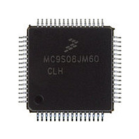
MC9S08JM60CLH Freescale, MC9S08JM60CLH Datasheet - Page 346

MC9S08JM60CLH
Manufacturer Part Number
MC9S08JM60CLH
Description
Manufacturer
Freescale
Datasheet
1.MC9S08JM60CLH.pdf
(388 pages)
Specifications of MC9S08JM60CLH
Cpu Family
HCS08
Device Core Size
8b
Frequency (max)
24MHz
Interface Type
SCI/SPI
Total Internal Ram Size
4KB
# I/os (max)
51
Number Of Timers - General Purpose
8
Operating Supply Voltage (typ)
3.3/5V
Operating Supply Voltage (max)
5.5V
Operating Supply Voltage (min)
2.7V
On-chip Adc
12-chx12-bit
Instruction Set Architecture
CISC
Operating Temp Range
-40C to 85C
Operating Temperature Classification
Industrial
Mounting
Surface Mount
Pin Count
64
Package Type
LQFP
Program Memory Type
Flash
Program Memory Size
60KB
Lead Free Status / RoHS Status
Compliant
Available stocks
Company
Part Number
Manufacturer
Quantity
Price
Company:
Part Number:
MC9S08JM60CLH
Manufacturer:
Freescale Semiconductor
Quantity:
10 000
Part Number:
MC9S08JM60CLH
Manufacturer:
FREESCALE
Quantity:
20 000
Company:
Part Number:
MC9S08JM60CLHE
Manufacturer:
AZBIL
Quantity:
1 000
- Current page: 346 of 388
- Download datasheet (5Mb)
Development Support
18.4.3.7
This register can be read or written at any time.
346
Reset
RWBEN
DBGEN
RWAEN
BRKEN
Field
ARM
RWA
RWB
TAG
W
7
6
5
4
3
2
1
0
R
DBGEN
Debug Module Enable — Used to enable the debug module. DBGEN cannot be set to 1 if the MCU is secure.
0 DBG disabled
1 DBG enabled
Arm Control — Controls whether the debugger is comparing and storing information in the FIFO. A write is used
to set this bit (and ARMF) and completion of a debug run automatically clears it. Any debug run can be manually
stopped by writing 0 to ARM or to DBGEN.
0 Debugger not armed
1 Debugger armed
Tag/Force Select — Controls whether break requests to the CPU will be tag or force type requests. If
BRKEN = 0, this bit has no meaning or effect.
0 CPU breaks requested as force type requests
1 CPU breaks requested as tag type requests
Break Enable — Controls whether a trigger event will generate a break request to the CPU. Trigger events can
cause information to be stored in the FIFO without generating a break request to the CPU. For an end trace, CPU
break requests are issued to the CPU when the comparator(s) and R/W meet the trigger requirements. For a
begin trace, CPU break requests are issued when the FIFO becomes full. TRGSEL does not affect the timing of
CPU break requests.
0 CPU break requests not enabled
1 Triggers cause a break request to the CPU
R/W Comparison Value for Comparator A — When RWAEN = 1, this bit determines whether a read or a write
access qualifies comparator A. When RWAEN = 0, RWA and the R/W signal do not affect comparator A.
0 Comparator A can only match on a write cycle
1 Comparator A can only match on a read cycle
Enable R/W for Comparator A — Controls whether the level of R/W is considered for a comparator A match.
0 R/W is not used in comparison A
1 R/W is used in comparison A
R/W Comparison Value for Comparator B — When RWBEN = 1, this bit determines whether a read or a write
access qualifies comparator B. When RWBEN = 0, RWB and the R/W signal do not affect comparator B.
0 Comparator B can match only on a write cycle
1 Comparator B can match only on a read cycle
Enable R/W for Comparator B — Controls whether the level of R/W is considered for a comparator B match.
0 R/W is not used in comparison B
1 R/W is used in comparison B
0
7
Debug Control Register (DBGC)
ARM
0
6
Table 18-4. DBGC Register Field Descriptions
Figure 18-7. Debug Control Register (DBGC)
MC9S08JM60 Series Data Sheet, Rev. 3
TAG
0
5
BRKEN
0
4
Description
RWA
0
3
RWAEN
0
2
Freescale Semiconductor
RWB
1
0
RWBEN
0
0
Related parts for MC9S08JM60CLH
Image
Part Number
Description
Manufacturer
Datasheet
Request
R

Part Number:
Description:
TOWER ELEVATOR BOARDS HARDWARE
Manufacturer:
Freescale Semiconductor
Datasheet:

Part Number:
Description:
TOWER SERIAL I/O HARDWARE
Manufacturer:
Freescale Semiconductor
Datasheet:

Part Number:
Description:
LCD MODULE FOR TWR SYSTEM
Manufacturer:
Freescale Semiconductor
Datasheet:

Part Number:
Description:
DAUGHTER LCD WVGA I.MX51
Manufacturer:
Freescale Semiconductor
Datasheet:

Part Number:
Description:
TOWER SYSTEM BOARD MPC5125
Manufacturer:
Freescale Semiconductor
Datasheet:

Part Number:
Description:
KIT EVALUATION I.MX51
Manufacturer:
Freescale Semiconductor
Datasheet:

Part Number:
Description:
KIT DEVELOPMENT WINCE IMX25
Manufacturer:
Freescale Semiconductor
Datasheet:

Part Number:
Description:
TOWER SYSTEM KIT MPC5125
Manufacturer:
Freescale Semiconductor
Datasheet:

Part Number:
Description:
TOWER SYSTEM BOARD K40X256
Manufacturer:
Freescale Semiconductor
Datasheet:

Part Number:
Description:
TOWER SYSTEM KIT K40X256
Manufacturer:
Freescale Semiconductor
Datasheet:

Part Number:
Description:
Microcontrollers (MCU) MX28 PLATFORM DEV KIT
Manufacturer:
Freescale Semiconductor
Datasheet:

Part Number:
Description:
MCU, MPU & DSP Development Tools IAR KickStart Kit for Kinetis K60
Manufacturer:
Freescale Semiconductor
Datasheet:

Part Number:
Description:
24BIT HDMI MX535/08
Manufacturer:
Freescale Semiconductor
Datasheet:
Part Number:
Description:
Manufacturer:
Freescale Semiconductor, Inc
Datasheet:
Part Number:
Description:
Manufacturer:
Freescale Semiconductor, Inc
Datasheet:


