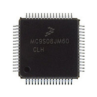
MC9S08JM60CLH Freescale, MC9S08JM60CLH Datasheet - Page 198

MC9S08JM60CLH
Manufacturer Part Number
MC9S08JM60CLH
Description
Manufacturer
Freescale
Datasheet
1.MC9S08JM60CLH.pdf
(388 pages)
Specifications of MC9S08JM60CLH
Cpu Family
HCS08
Device Core Size
8b
Frequency (max)
24MHz
Interface Type
SCI/SPI
Total Internal Ram Size
4KB
# I/os (max)
51
Number Of Timers - General Purpose
8
Operating Supply Voltage (typ)
3.3/5V
Operating Supply Voltage (max)
5.5V
Operating Supply Voltage (min)
2.7V
On-chip Adc
12-chx12-bit
Instruction Set Architecture
CISC
Operating Temp Range
-40C to 85C
Operating Temperature Classification
Industrial
Mounting
Surface Mount
Pin Count
64
Package Type
LQFP
Program Memory Type
Flash
Program Memory Size
60KB
Lead Free Status / RoHS Status
Compliant
Available stocks
Company
Part Number
Manufacturer
Quantity
Price
Company:
Part Number:
MC9S08JM60CLH
Manufacturer:
Freescale Semiconductor
Quantity:
10 000
Part Number:
MC9S08JM60CLH
Manufacturer:
FREESCALE
Quantity:
20 000
Company:
Part Number:
MC9S08JM60CLHE
Manufacturer:
AZBIL
Quantity:
1 000
- Current page: 198 of 388
- Download datasheet (5Mb)
Multi-Purpose Clock Generator (S08MCGV1)
BDIV=01 (divide by 2), RDIV < 011
12.5
This section describes how to initialize and configure the MCG module in application. The following
sections include examples on how to initialize the MCG and properly switch between the various available
modes.
12.5.1
The MCG comes out of reset configured for FEI mode with the BDIV set for divide-by-2. The internal
reference will stabilize in t
reference is stable, the FLL will acquire lock in t
Upon POR, the internal reference will require trimming to guarantee an accurate clock. Freescale
recommends using FLASH location 0xFFAE for storing the fine trim bit, FTRIM in the MCGSC register,
and 0xFFAF for storing the 8-bit trim value in the MCGTRM register. The MCU will not automatically
copy the values in these FLASH locations to the respective registers. Therefore, user code must copy these
values from FLASH to the registers.
12.5.1.1
Because the MCG comes out of reset in FEI mode, the only MCG modes which can be directly switched
to upon reset are FEE, FBE, and FBI modes (see
first configuring the MCG for one of these three initial modes. Care must be taken to check relevant status
bits in the MCGSC register reflecting all configuration changes within each mode.
To change from FEI mode to FEE or FBE modes, follow this procedure:
198
1. Enable the external clock source by setting the appropriate bits in MCGC2.
2. Write to MCGC1 to select the clock mode.
— If entering FEE, set RDIV appropriately, clear the IREFS bit to switch to the external reference,
— If entering FBE, clear the IREFS bit to switch to the external reference and change the CLKS
— The internal reference can optionally be kept running by setting the IRCLKEN bit. This is
Initialization / Application Information
and leave the CLKS bits at %00 so that the output of the FLL is selected as the system clock
source.
bits to %10 so that the external reference clock is selected as the system clock source. The
RDIV bits should also be set appropriately here according to the external reference frequency
because although the FLL is bypassed, it is still on in FBE mode.
useful if the application will switch back and forth between internal and external modes. For
MCG Module Initialization Sequence
Initializing the MCG
•
The BDIV value should not be changed to divide-by-1 without first
trimming the internal reference. Failure to do so could result in the MCU
running out of specification.
BDIV=00 (divide by 1), RDIV < 010
irefst
microseconds before the FLL can acquire lock. As soon as the internal
MC9S08JM60 Series Data Sheet, Rev. 3
fll_lock
NOTE
Figure
milliseconds.
12-8). Reaching any of the other modes requires
Freescale Semiconductor
Related parts for MC9S08JM60CLH
Image
Part Number
Description
Manufacturer
Datasheet
Request
R

Part Number:
Description:
TOWER ELEVATOR BOARDS HARDWARE
Manufacturer:
Freescale Semiconductor
Datasheet:

Part Number:
Description:
TOWER SERIAL I/O HARDWARE
Manufacturer:
Freescale Semiconductor
Datasheet:

Part Number:
Description:
LCD MODULE FOR TWR SYSTEM
Manufacturer:
Freescale Semiconductor
Datasheet:

Part Number:
Description:
DAUGHTER LCD WVGA I.MX51
Manufacturer:
Freescale Semiconductor
Datasheet:

Part Number:
Description:
TOWER SYSTEM BOARD MPC5125
Manufacturer:
Freescale Semiconductor
Datasheet:

Part Number:
Description:
KIT EVALUATION I.MX51
Manufacturer:
Freescale Semiconductor
Datasheet:

Part Number:
Description:
KIT DEVELOPMENT WINCE IMX25
Manufacturer:
Freescale Semiconductor
Datasheet:

Part Number:
Description:
TOWER SYSTEM KIT MPC5125
Manufacturer:
Freescale Semiconductor
Datasheet:

Part Number:
Description:
TOWER SYSTEM BOARD K40X256
Manufacturer:
Freescale Semiconductor
Datasheet:

Part Number:
Description:
TOWER SYSTEM KIT K40X256
Manufacturer:
Freescale Semiconductor
Datasheet:

Part Number:
Description:
Microcontrollers (MCU) MX28 PLATFORM DEV KIT
Manufacturer:
Freescale Semiconductor
Datasheet:

Part Number:
Description:
MCU, MPU & DSP Development Tools IAR KickStart Kit for Kinetis K60
Manufacturer:
Freescale Semiconductor
Datasheet:

Part Number:
Description:
24BIT HDMI MX535/08
Manufacturer:
Freescale Semiconductor
Datasheet:
Part Number:
Description:
Manufacturer:
Freescale Semiconductor, Inc
Datasheet:
Part Number:
Description:
Manufacturer:
Freescale Semiconductor, Inc
Datasheet:


