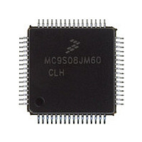
MC9S08JM60CLH Freescale, MC9S08JM60CLH Datasheet - Page 257

MC9S08JM60CLH
Manufacturer Part Number
MC9S08JM60CLH
Description
Manufacturer
Freescale
Datasheet
1.MC9S08JM60CLH.pdf
(388 pages)
Specifications of MC9S08JM60CLH
Cpu Family
HCS08
Device Core Size
8b
Frequency (max)
24MHz
Interface Type
SCI/SPI
Total Internal Ram Size
4KB
# I/os (max)
51
Number Of Timers - General Purpose
8
Operating Supply Voltage (typ)
3.3/5V
Operating Supply Voltage (max)
5.5V
Operating Supply Voltage (min)
2.7V
On-chip Adc
12-chx12-bit
Instruction Set Architecture
CISC
Operating Temp Range
-40C to 85C
Operating Temperature Classification
Industrial
Mounting
Surface Mount
Pin Count
64
Package Type
LQFP
Program Memory Type
Flash
Program Memory Size
60KB
Lead Free Status / RoHS Status
Compliant
Available stocks
Company
Part Number
Manufacturer
Quantity
Price
Company:
Part Number:
MC9S08JM60CLH
Manufacturer:
Freescale Semiconductor
Quantity:
10 000
Part Number:
MC9S08JM60CLH
Manufacturer:
FREESCALE
Quantity:
20 000
Company:
Part Number:
MC9S08JM60CLHE
Manufacturer:
AZBIL
Quantity:
1 000
- Current page: 257 of 388
- Download datasheet (5Mb)
and SPSCK lines. In this case, the SPI immediately switches to slave mode, by clearing the MSTR bit and
also disables the slave output buffer MISO (or SISO in bidirectional mode). So the result is that all outputs
are disabled and SPSCK, MOSI and MISO are inputs. If a transmission is in progress when the mode fault
occurs, the transmission is aborted and the SPI is forced into idle state.
This mode fault error also sets the mode fault (MODF) flag in the SPI Status Register (SPIxS). If the SPI
interrupt enable bit (SPIE) is set when the MODF flag gets set, then an SPI interrupt sequence is also
requested.
When a write to the SPI Data Register in the master occurs, there is a half SPSCK-cycle delay. After the
delay, SPSCK is started within the master. The rest of the transfer operation differs slightly, depending on
the clock format specified by the SPI clock phase bit, CPHA, in SPI Control Register 1 (see
“SPI Clock
15.4.3
The SPI operates in slave mode when the MSTR bit in SPI Control Register1 is clear.
In slave mode, SPSCK is the SPI clock input from the master.
In slave mode, the function of the serial data output pin (MISO) and serial data input pin (MOSI) is
determined by the SPC0 bit and BIDIROE bit in SPI Control Register 2.
be low. SS must remain low until the transmission is complete. If SS goes high, the SPI is forced into idle
state.
is high impedance, and, if SS is low the first bit in the SPI Data Register is driven out of the serial data
output pin. Also, if the slave is not selected (SS is high), then the SPSCK input is ignored and no internal
shifting of the SPI shift register takes place.
Although the SPI is capable of duplex operation, some SPI peripherals are capable of only receiving SPI
data in a slave mode. For these simpler devices, there is no serial data out pin.
Freescale Semiconductor
The SS input also controls the serial data output pin, if SS is high (not selected), the serial data output pin
The SS pin is the slave select input. Before a data transmission occurs, the SS pin of the slave SPI must
•
•
•
SPSCK
MISO, MOSI pin
SS pin
Formats.”)
Slave Mode
A change of the bits CPOL, CPHA, SSOE, LSBFE, MODFEN, SPC0,
BIDIROE with SPC0 set, SPIMODE, SPPR2-SPPR0 and SPR2-SPR0 in
master mode will abort a transmission in progress and force the SPI into idle
state. The remote slave cannot detect this, therefore the master has to ensure
that the remote slave is set back to idle state.
MC9S08JM60 Series Data Sheet, Rev. 3
NOTE
Serial Peripheral Interface (S08SPI16V1)
Section 15.4.5,
257
Related parts for MC9S08JM60CLH
Image
Part Number
Description
Manufacturer
Datasheet
Request
R

Part Number:
Description:
TOWER ELEVATOR BOARDS HARDWARE
Manufacturer:
Freescale Semiconductor
Datasheet:

Part Number:
Description:
TOWER SERIAL I/O HARDWARE
Manufacturer:
Freescale Semiconductor
Datasheet:

Part Number:
Description:
LCD MODULE FOR TWR SYSTEM
Manufacturer:
Freescale Semiconductor
Datasheet:

Part Number:
Description:
DAUGHTER LCD WVGA I.MX51
Manufacturer:
Freescale Semiconductor
Datasheet:

Part Number:
Description:
TOWER SYSTEM BOARD MPC5125
Manufacturer:
Freescale Semiconductor
Datasheet:

Part Number:
Description:
KIT EVALUATION I.MX51
Manufacturer:
Freescale Semiconductor
Datasheet:

Part Number:
Description:
KIT DEVELOPMENT WINCE IMX25
Manufacturer:
Freescale Semiconductor
Datasheet:

Part Number:
Description:
TOWER SYSTEM KIT MPC5125
Manufacturer:
Freescale Semiconductor
Datasheet:

Part Number:
Description:
TOWER SYSTEM BOARD K40X256
Manufacturer:
Freescale Semiconductor
Datasheet:

Part Number:
Description:
TOWER SYSTEM KIT K40X256
Manufacturer:
Freescale Semiconductor
Datasheet:

Part Number:
Description:
Microcontrollers (MCU) MX28 PLATFORM DEV KIT
Manufacturer:
Freescale Semiconductor
Datasheet:

Part Number:
Description:
MCU, MPU & DSP Development Tools IAR KickStart Kit for Kinetis K60
Manufacturer:
Freescale Semiconductor
Datasheet:

Part Number:
Description:
24BIT HDMI MX535/08
Manufacturer:
Freescale Semiconductor
Datasheet:
Part Number:
Description:
Manufacturer:
Freescale Semiconductor, Inc
Datasheet:
Part Number:
Description:
Manufacturer:
Freescale Semiconductor, Inc
Datasheet:


