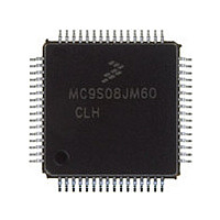
MC9S08JM60CLH Freescale, MC9S08JM60CLH Datasheet - Page 158

MC9S08JM60CLH
Manufacturer Part Number
MC9S08JM60CLH
Description
Manufacturer
Freescale
Datasheet
1.MC9S08JM60CLH.pdf
(388 pages)
Specifications of MC9S08JM60CLH
Cpu Family
HCS08
Device Core Size
8b
Frequency (max)
24MHz
Interface Type
SCI/SPI
Total Internal Ram Size
4KB
# I/os (max)
51
Number Of Timers - General Purpose
8
Operating Supply Voltage (typ)
3.3/5V
Operating Supply Voltage (max)
5.5V
Operating Supply Voltage (min)
2.7V
On-chip Adc
12-chx12-bit
Instruction Set Architecture
CISC
Operating Temp Range
-40C to 85C
Operating Temperature Classification
Industrial
Mounting
Surface Mount
Pin Count
64
Package Type
LQFP
Program Memory Type
Flash
Program Memory Size
60KB
Lead Free Status / RoHS Status
Compliant
Available stocks
Company
Part Number
Manufacturer
Quantity
Price
Company:
Part Number:
MC9S08JM60CLH
Manufacturer:
Freescale Semiconductor
Quantity:
10 000
Part Number:
MC9S08JM60CLH
Manufacturer:
FREESCALE
Quantity:
20 000
Company:
Part Number:
MC9S08JM60CLHE
Manufacturer:
AZBIL
Quantity:
1 000
- Current page: 158 of 388
- Download datasheet (5Mb)
Analog-to-Digital Converter (S08ADC12V1)
For proper conversion, the input voltage must fall between V
exceeds V
(full scale 10-bit representation) or 0xFF (full scale 8-bit representation). If the input is equal to or less
than V
straight-line linear conversions. There is a brief current associated with V
capacitor is charging. The input is sampled for 3.5 cycles of the ADCK source when ADLSMP is low, or
23.5 cycles when ADLSMP is high.
For minimal loss of accuracy due to current injection, pins adjacent to the analog input pins should not be
transitioning during conversions.
10.6.2
Several sources of error exist for A/D conversions. These are discussed in the following sections.
10.6.2.1
For proper conversions, the input must be sampled long enough to achieve the proper accuracy. Given the
maximum input resistance of approximately 7kΩ and input capacitance of approximately 5.5 pF, sampling
to within 1/4
8 MHz maximum ADCK frequency) provided the resistance of the external analog source (R
below 2 kΩ.
Higher source resistances or higher-accuracy sampling is possible by setting ADLSMP (to increase the
sample window to 23.5 cycles) or decreasing ADCK frequency to increase sample time.
10.6.2.2
Leakage on the I/O pins can cause conversion error if the external analog source resistance (R
If this error cannot be tolerated by the application, keep R
1/4
10.6.2.3
System noise that occurs during the sample or conversion process can affect the accuracy of the
conversion. The ADC accuracy numbers are guaranteed as specified only if the following conditions are
met:
158
LSB
•
•
•
•
•
REFL
leakage error (N = 8 in 8-bit, 10 in 10-bit or 12 in 12-bit mode).
There is a 0.1 μF low-ESR capacitor from V
There is a 0.1 μF low-ESR capacitor from V
If inductive isolation is used from the primary supply, an additional 1 μF capacitor is placed from
V
V
Operate the MCU in wait or stop3 mode before initiating (hardware triggered conversions) or
immediately after initiating (hardware or software triggered conversions) the ADC conversion.
— For software triggered conversions, immediately follow the write to ADCSC1 with a wait
DDAD
SSAD
REFH
instruction or stop instruction.
, the converter circuit converts it to 0x000. Input voltages between V
Sources of Error
LSB
Sampling Error
Pin Leakage Error
Noise-Induced Errors
(and V
, the converter circuit converts the signal to 0xFFF (full scale 12-bit representation), 0x3FF
to V
(at 12-bit resolution) can be achieved within the minimum sample window (3.5 cycles @
SSAD
REFL
.
, if connected) is connected to V
MC9S08JM60 Series Data Sheet, Rev. 3
REFH
DDAD
AS
to V
to V
SS
lower than V
REFH
at a quiet point in the ground plane.
REFL
SSAD
and V
.
.
DDAD
REFL
REFL
. If the input is equal to or
when the sampling
/ (2
REFH
N
*I
Freescale Semiconductor
LEAK
and V
) for less than
REFL
AS
AS
) is kept
) is high.
are
Related parts for MC9S08JM60CLH
Image
Part Number
Description
Manufacturer
Datasheet
Request
R

Part Number:
Description:
TOWER ELEVATOR BOARDS HARDWARE
Manufacturer:
Freescale Semiconductor
Datasheet:

Part Number:
Description:
TOWER SERIAL I/O HARDWARE
Manufacturer:
Freescale Semiconductor
Datasheet:

Part Number:
Description:
LCD MODULE FOR TWR SYSTEM
Manufacturer:
Freescale Semiconductor
Datasheet:

Part Number:
Description:
DAUGHTER LCD WVGA I.MX51
Manufacturer:
Freescale Semiconductor
Datasheet:

Part Number:
Description:
TOWER SYSTEM BOARD MPC5125
Manufacturer:
Freescale Semiconductor
Datasheet:

Part Number:
Description:
KIT EVALUATION I.MX51
Manufacturer:
Freescale Semiconductor
Datasheet:

Part Number:
Description:
KIT DEVELOPMENT WINCE IMX25
Manufacturer:
Freescale Semiconductor
Datasheet:

Part Number:
Description:
TOWER SYSTEM KIT MPC5125
Manufacturer:
Freescale Semiconductor
Datasheet:

Part Number:
Description:
TOWER SYSTEM BOARD K40X256
Manufacturer:
Freescale Semiconductor
Datasheet:

Part Number:
Description:
TOWER SYSTEM KIT K40X256
Manufacturer:
Freescale Semiconductor
Datasheet:

Part Number:
Description:
Microcontrollers (MCU) MX28 PLATFORM DEV KIT
Manufacturer:
Freescale Semiconductor
Datasheet:

Part Number:
Description:
MCU, MPU & DSP Development Tools IAR KickStart Kit for Kinetis K60
Manufacturer:
Freescale Semiconductor
Datasheet:

Part Number:
Description:
24BIT HDMI MX535/08
Manufacturer:
Freescale Semiconductor
Datasheet:
Part Number:
Description:
Manufacturer:
Freescale Semiconductor, Inc
Datasheet:
Part Number:
Description:
Manufacturer:
Freescale Semiconductor, Inc
Datasheet:


