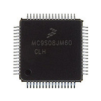
MC9S08JM60CLH Freescale, MC9S08JM60CLH Datasheet - Page 234

MC9S08JM60CLH
Manufacturer Part Number
MC9S08JM60CLH
Description
Manufacturer
Freescale
Datasheet
1.MC9S08JM60CLH.pdf
(388 pages)
Specifications of MC9S08JM60CLH
Cpu Family
HCS08
Device Core Size
8b
Frequency (max)
24MHz
Interface Type
SCI/SPI
Total Internal Ram Size
4KB
# I/os (max)
51
Number Of Timers - General Purpose
8
Operating Supply Voltage (typ)
3.3/5V
Operating Supply Voltage (max)
5.5V
Operating Supply Voltage (min)
2.7V
On-chip Adc
12-chx12-bit
Instruction Set Architecture
CISC
Operating Temp Range
-40C to 85C
Operating Temperature Classification
Industrial
Mounting
Surface Mount
Pin Count
64
Package Type
LQFP
Program Memory Type
Flash
Program Memory Size
60KB
Lead Free Status / RoHS Status
Compliant
Available stocks
Company
Part Number
Manufacturer
Quantity
Price
Company:
Part Number:
MC9S08JM60CLH
Manufacturer:
Freescale Semiconductor
Quantity:
10 000
Part Number:
MC9S08JM60CLH
Manufacturer:
FREESCALE
Quantity:
20 000
Company:
Part Number:
MC9S08JM60CLHE
Manufacturer:
AZBIL
Quantity:
1 000
- Current page: 234 of 388
- Download datasheet (5Mb)
Serial Communications Interface (S08SCIV4)
1
When using an internal oscillator in a LIN system, it is necessary to raise the break detection threshold by
one bit time. Under the worst case timing conditions allowed in LIN, it is possible that a 0x00 data
character can appear to be 10.26 bit times long at a slave which is running 14% faster than the master. This
would trigger normal break detection circuitry which is designed to detect a 10 bit break symbol. When
the LBKDE bit is set, framing errors are inhibited and the break detection threshold changes from 10 bits
to 11 bits, preventing false detection of a 0x00 data character as a LIN break symbol.
14.2.6
234
Setting RXINV inverts the RxD input for all cases: data bits, start and stop bits, break, and idle.
Reset
LBKDE
TXDIR
Field
Field
RAF
R8
T8
1
0
7
6
5
W
R
SCI Control Register 3 (SCIxC3)
LIN Break Detection Enable— LBKDE is used to select a longer break character detection length. While LBKDE
is set, framing error (FE) and receive data register full (RDRF) flags are prevented from setting.
0 Break character is detected at length of 10 bit times (11 if M = 1).
1 Break character is detected at length of 11 bit times (12 if M = 1).
Receiver Active Flag — RAF is set when the SCI receiver detects the beginning of a valid start bit, and RAF is
cleared automatically when the receiver detects an idle line. This status flag can be used to check whether an
SCI character is being received before instructing the MCU to go to stop mode.
0 SCI receiver idle waiting for a start bit.
1 SCI receiver active (RxD input not idle).
Ninth Data Bit for Receiver — When the SCI is configured for 9-bit data (M = 1), R8 can be thought of as a ninth
receive data bit to the left of the MSB of the buffered data in the SCIxD register. When reading 9-bit data, read
R8 before reading SCIxD because reading SCIxD completes automatic flag clearing sequences which could
allow R8 and SCIxD to be overwritten with new data.
Ninth Data Bit for Transmitter — When the SCI is configured for 9-bit data (M = 1), T8 may be thought of as a
ninth transmit data bit to the left of the MSB of the data in the SCIxD register. When writing 9-bit data, the entire
9-bit value is transferred to the SCI shift register after SCIxD is written so T8 should be written (if it needs to
change from its previous value) before SCIxD is written. If T8 does not need to change in the new value (such
as when it is used to generate mark or space parity), it need not be written each time SCIxD is written.
TxD Pin Direction in Single-Wire Mode — When the SCI is configured for single-wire half-duplex operation
(LOOPS = RSRC = 1), this bit determines the direction of data at the TxD pin.
0 TxD pin is an input in single-wire mode.
1 TxD pin is an output in single-wire mode.
R8
0
7
= Unimplemented or Reserved
T8
0
6
Table 14-6. SCIxS2 Field Descriptions (continued)
Figure 14-10. SCI Control Register 3 (SCIxC3)
Table 14-7. SCIxC3 Field Descriptions
MC9S08JM60 Series Data Sheet, Rev. 3
TXDIR
0
5
TXINV
0
4
Description
Description
ORIE
3
0
NEIE
0
2
Freescale Semiconductor
FEIE
0
1
PEIE
0
0
Related parts for MC9S08JM60CLH
Image
Part Number
Description
Manufacturer
Datasheet
Request
R

Part Number:
Description:
TOWER ELEVATOR BOARDS HARDWARE
Manufacturer:
Freescale Semiconductor
Datasheet:

Part Number:
Description:
TOWER SERIAL I/O HARDWARE
Manufacturer:
Freescale Semiconductor
Datasheet:

Part Number:
Description:
LCD MODULE FOR TWR SYSTEM
Manufacturer:
Freescale Semiconductor
Datasheet:

Part Number:
Description:
DAUGHTER LCD WVGA I.MX51
Manufacturer:
Freescale Semiconductor
Datasheet:

Part Number:
Description:
TOWER SYSTEM BOARD MPC5125
Manufacturer:
Freescale Semiconductor
Datasheet:

Part Number:
Description:
KIT EVALUATION I.MX51
Manufacturer:
Freescale Semiconductor
Datasheet:

Part Number:
Description:
KIT DEVELOPMENT WINCE IMX25
Manufacturer:
Freescale Semiconductor
Datasheet:

Part Number:
Description:
TOWER SYSTEM KIT MPC5125
Manufacturer:
Freescale Semiconductor
Datasheet:

Part Number:
Description:
TOWER SYSTEM BOARD K40X256
Manufacturer:
Freescale Semiconductor
Datasheet:

Part Number:
Description:
TOWER SYSTEM KIT K40X256
Manufacturer:
Freescale Semiconductor
Datasheet:

Part Number:
Description:
Microcontrollers (MCU) MX28 PLATFORM DEV KIT
Manufacturer:
Freescale Semiconductor
Datasheet:

Part Number:
Description:
MCU, MPU & DSP Development Tools IAR KickStart Kit for Kinetis K60
Manufacturer:
Freescale Semiconductor
Datasheet:

Part Number:
Description:
24BIT HDMI MX535/08
Manufacturer:
Freescale Semiconductor
Datasheet:
Part Number:
Description:
Manufacturer:
Freescale Semiconductor, Inc
Datasheet:
Part Number:
Description:
Manufacturer:
Freescale Semiconductor, Inc
Datasheet:


