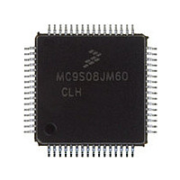
MC9S08JM60CLH Freescale, MC9S08JM60CLH Datasheet - Page 363

MC9S08JM60CLH
Manufacturer Part Number
MC9S08JM60CLH
Description
Manufacturer
Freescale
Datasheet
1.MC9S08JM60CLH.pdf
(388 pages)
Specifications of MC9S08JM60CLH
Cpu Family
HCS08
Device Core Size
8b
Frequency (max)
24MHz
Interface Type
SCI/SPI
Total Internal Ram Size
4KB
# I/os (max)
51
Number Of Timers - General Purpose
8
Operating Supply Voltage (typ)
3.3/5V
Operating Supply Voltage (max)
5.5V
Operating Supply Voltage (min)
2.7V
On-chip Adc
12-chx12-bit
Instruction Set Architecture
CISC
Operating Temp Range
-40C to 85C
Operating Temperature Classification
Industrial
Mounting
Surface Mount
Pin Count
64
Package Type
LQFP
Program Memory Type
Flash
Program Memory Size
60KB
Lead Free Status / RoHS Status
Compliant
Available stocks
Company
Part Number
Manufacturer
Quantity
Price
Company:
Part Number:
MC9S08JM60CLH
Manufacturer:
Freescale Semiconductor
Quantity:
10 000
Part Number:
MC9S08JM60CLH
Manufacturer:
FREESCALE
Quantity:
20 000
Company:
Part Number:
MC9S08JM60CLHE
Manufacturer:
AZBIL
Quantity:
1 000
- Current page: 363 of 388
- Download datasheet (5Mb)
1
2
3
Num C
A.11 MCG Specifications
Freescale Semiconductor
10
11
12
13
14
15
16
17
18
19
20
21
22
23
1
2
3
4
5
6
7
8
9
TRIM register at default value (0x80) and FTRIM control bit at default value (0x0).
This specification applies to any time the FLL reference source or reference divider is changed, trim value changed or changing
from FLL disabled (BLPE, BLPI) to FLL enabled (FEI, FEE, FBE, FBI). If a crystal/resonator is being used as the reference, this
specification assumes it is already running.
This specification applies to any time the PLL VCO divider or reference divider is changed, or changing from PLL disabled (BLPE,
BLPI) to PLL enabled (PBE, PEE). If a crystal/resonator is being used as the reference, this specification assumes it is already
running.
—
P
P Average internal reference frequency – untrimmed
P Average internal reference frequency Q – user trimmed
D Internal reference startup time
P DCO output frequency range - trimmed
C
C
P
C
C FLL acquisition time
D PLL acquisition time
C
D VCO operating frequency
D PLL reference frequency range
D Lock entry frequency tolerance
D Lock exit frequency tolerance
D Lock time – FLL
D Lock time – PLL
D Loss of external clock minimum frequency – RANGE = 0
D Loss of external clock minimum frequency – RANGE = 1
T
T Jitter of PLL output clock measured over 625 ns
Internal reference frequency - factory trimmed at V
5 V and temperature = 25
DCO output frequency range - untrimmed
value provided for reference: f
Resolution of trimmed DCO output frequency at fixed
voltage and temperature (using FTRIM)
Resolution of trimmed DCO output frequency at fixed
voltage and temperature (not using FTRIM)
Total deviation of trimmed DCO output frequency over
voltage and temperature
Total deviation of trimmed DCO output frequency over
fixed voltage and temperature range of 0 –70
Long term Jitter of DCO output clock (averaged over
2ms interval)
Long term accuracy of PLL output clock (averaged over
2 ms)
Table A-12. MCG Frequency Specifications (Temperature Range = –40 to 125°C Ambient)
4
2
3
Rating
°C
dco_ut
7
6
MC9S08JM60 Series Data Sheet, Rev. 3
= 1024 X f
1
°C
int_ut
DD
1
=
f
pll_jitter_625ns
f
pll_jitter_2ms
Δf
Δf
t
t
Symbol
pll_acquire
fll_acquire
f
Δf
Δf
t
f
t
f
dco_res_t
dco_res_t
loc_high
C
f
pll_lock
loc_low
f
f
dco_ut
D
fll_lock
f
t
f
pll_ref
D
int_ut
dco_t
f
int_ft
irefst
int_t
dco_t
dco_t
Jitter
vco
lock
unl
(16/5) x f
(3/5) x f
31.25
±1.49
±4.47
25.6
Min
7.0
1.0
25
32
—
—
—
—
—
—
—
—
—
—
—
—
—
int
int
Appendix A Electrical Characteristics
Typical
0.590
0.566
31.25
33.48
32.7
±0.1
±0.2
+0.5
–1.0
±0.5
0.02
60
—
—
—
—
—
—
—
—
—
—
—
—
5
5
1075(1/
1075(1/
t
t
pll_acquire+
fll_acquire+
39.0625
41.66
42.66
±2.98
±5.97
Max
±0.2
±0.4
55.0
100
0.2
2.0
40
±2
±1
—
—
—
—
—
1
1
f
f
pll_ref)
int_t)
%f
%f
%f
%f
%f
MHz
MHz
MHz
MHz
Unit
%f
%f
kHz
kHz
kHz
kHz
kHz
ms
ms
μs
%
%
363
s
s
dco
dco
dco
dco
dco
pll
pll
Related parts for MC9S08JM60CLH
Image
Part Number
Description
Manufacturer
Datasheet
Request
R

Part Number:
Description:
TOWER ELEVATOR BOARDS HARDWARE
Manufacturer:
Freescale Semiconductor
Datasheet:

Part Number:
Description:
TOWER SERIAL I/O HARDWARE
Manufacturer:
Freescale Semiconductor
Datasheet:

Part Number:
Description:
LCD MODULE FOR TWR SYSTEM
Manufacturer:
Freescale Semiconductor
Datasheet:

Part Number:
Description:
DAUGHTER LCD WVGA I.MX51
Manufacturer:
Freescale Semiconductor
Datasheet:

Part Number:
Description:
TOWER SYSTEM BOARD MPC5125
Manufacturer:
Freescale Semiconductor
Datasheet:

Part Number:
Description:
KIT EVALUATION I.MX51
Manufacturer:
Freescale Semiconductor
Datasheet:

Part Number:
Description:
KIT DEVELOPMENT WINCE IMX25
Manufacturer:
Freescale Semiconductor
Datasheet:

Part Number:
Description:
TOWER SYSTEM KIT MPC5125
Manufacturer:
Freescale Semiconductor
Datasheet:

Part Number:
Description:
TOWER SYSTEM BOARD K40X256
Manufacturer:
Freescale Semiconductor
Datasheet:

Part Number:
Description:
TOWER SYSTEM KIT K40X256
Manufacturer:
Freescale Semiconductor
Datasheet:

Part Number:
Description:
Microcontrollers (MCU) MX28 PLATFORM DEV KIT
Manufacturer:
Freescale Semiconductor
Datasheet:

Part Number:
Description:
MCU, MPU & DSP Development Tools IAR KickStart Kit for Kinetis K60
Manufacturer:
Freescale Semiconductor
Datasheet:

Part Number:
Description:
24BIT HDMI MX535/08
Manufacturer:
Freescale Semiconductor
Datasheet:
Part Number:
Description:
Manufacturer:
Freescale Semiconductor, Inc
Datasheet:
Part Number:
Description:
Manufacturer:
Freescale Semiconductor, Inc
Datasheet:


