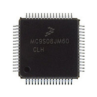
MC9S08JM60CLH Freescale, MC9S08JM60CLH Datasheet - Page 290

MC9S08JM60CLH
Manufacturer Part Number
MC9S08JM60CLH
Description
Manufacturer
Freescale
Datasheet
1.MC9S08JM60CLH.pdf
(388 pages)
Specifications of MC9S08JM60CLH
Cpu Family
HCS08
Device Core Size
8b
Frequency (max)
24MHz
Interface Type
SCI/SPI
Total Internal Ram Size
4KB
# I/os (max)
51
Number Of Timers - General Purpose
8
Operating Supply Voltage (typ)
3.3/5V
Operating Supply Voltage (max)
5.5V
Operating Supply Voltage (min)
2.7V
On-chip Adc
12-chx12-bit
Instruction Set Architecture
CISC
Operating Temp Range
-40C to 85C
Operating Temperature Classification
Industrial
Mounting
Surface Mount
Pin Count
64
Package Type
LQFP
Program Memory Type
Flash
Program Memory Size
60KB
Lead Free Status / RoHS Status
Compliant
Available stocks
Company
Part Number
Manufacturer
Quantity
Price
Company:
Part Number:
MC9S08JM60CLH
Manufacturer:
Freescale Semiconductor
Quantity:
10 000
Part Number:
MC9S08JM60CLH
Manufacturer:
FREESCALE
Quantity:
20 000
Company:
Part Number:
MC9S08JM60CLHE
Manufacturer:
AZBIL
Quantity:
1 000
- Current page: 290 of 388
- Download datasheet (5Mb)
Timer/PWM Module (S08TPMV3)
When the channel value register is set to 0x0000, the duty cycle is 0%. 100% duty cycle can be achieved
by setting the timer-channel register (TPMxCnVH:TPMxCnVL) to a value greater than the modulus
setting. This implies that the modulus setting must be less than 0xFFFF in order to get 100% duty cycle.
Because the TPM may be used in an 8-bit MCU, the settings in the timer channel registers are buffered to
ensure coherent 16-bit updates and to avoid unexpected PWM pulse widths. Writes to any of the registers
TPMxCnVH and TPMxCnVL, actually write to buffer registers. In edge-aligned PWM mode, values are
transferred to the corresponding timer-channel registers according to the value of CLKSB:CLKSA bits, so:
16.4.2.4
This type of PWM output uses the up/down counting mode of the timer counter (CPWMS=1). The output
compare value in TPMxCnVH:TPMxCnVL determines the pulse width (duty cycle) of the PWM signal
while the period is determined by the value in TPMxMODH:TPMxMODL. TPMxMODH:TPMxMODL
should be kept in the range of 0x0001 to 0x7FFF because values outside this range can produce ambiguous
results. ELSnA will determine the polarity of the CPWM output.
If the channel-value register TPMxCnVH:TPMxCnVL is zero or negative (bit 15 set), the duty cycle will
be 0%. If TPMxCnVH:TPMxCnVL is a positive value (bit 15 clear) and is greater than the (non-zero)
modulus setting, the duty cycle will be 100% because the duty cycle compare will never occur. This
implies the usable range of periods set by the modulus register is 0x0001 through 0x7FFE (0x7FFF if you
do not need to generate 100% duty cycle). This is not a significant limitation. The resulting period would
be much longer than required for normal applications.
TPMxMODH:TPMxMODL=0x0000 is a special case that should not be used with center-aligned PWM
mode. When CPWMS=0, this case corresponds to the counter running free from 0x0000 through 0xFFFF,
but when CPWMS=1 the counter needs a valid match to the modulus register somewhere other than at
0x0000 in order to change directions from up-counting to down-counting.
290
•
•
If (CLKSB:CLKSA = 0:0), the registers are updated when the second byte is written
If (CLKSB:CLKSA not = 0:0), the registers are updated after the both bytes were written, and the
TPM counter changes from (TPMxMODH:TPMxMODL - 1) to (TPMxMODH:TPMxMODL). If
the TPM counter is a free-running counter then the update is made when the TPM counter changes
from 0xFFFE to 0xFFFF.
pulse width = 2 x (TPMxCnVH:TPMxCnVL)
period = 2 x (TPMxMODH:TPMxMODL); TPMxMODH:TPMxMODL=0x0001-0x7FFF
TPMxCHn
Center-Aligned PWM Mode
OVERFLOW
Figure 16-15. PWM Period and Pulse Width (ELSnA=0)
PULSE
WIDTH
PERIOD
MC9S08JM60 Series Data Sheet, Rev. 3
COMPARE
OUTPUT
OVERFLOW
COMPARE
OUTPUT
OVERFLOW
COMPARE
OUTPUT
Freescale Semiconductor
Related parts for MC9S08JM60CLH
Image
Part Number
Description
Manufacturer
Datasheet
Request
R

Part Number:
Description:
TOWER ELEVATOR BOARDS HARDWARE
Manufacturer:
Freescale Semiconductor
Datasheet:

Part Number:
Description:
TOWER SERIAL I/O HARDWARE
Manufacturer:
Freescale Semiconductor
Datasheet:

Part Number:
Description:
LCD MODULE FOR TWR SYSTEM
Manufacturer:
Freescale Semiconductor
Datasheet:

Part Number:
Description:
DAUGHTER LCD WVGA I.MX51
Manufacturer:
Freescale Semiconductor
Datasheet:

Part Number:
Description:
TOWER SYSTEM BOARD MPC5125
Manufacturer:
Freescale Semiconductor
Datasheet:

Part Number:
Description:
KIT EVALUATION I.MX51
Manufacturer:
Freescale Semiconductor
Datasheet:

Part Number:
Description:
KIT DEVELOPMENT WINCE IMX25
Manufacturer:
Freescale Semiconductor
Datasheet:

Part Number:
Description:
TOWER SYSTEM KIT MPC5125
Manufacturer:
Freescale Semiconductor
Datasheet:

Part Number:
Description:
TOWER SYSTEM BOARD K40X256
Manufacturer:
Freescale Semiconductor
Datasheet:

Part Number:
Description:
TOWER SYSTEM KIT K40X256
Manufacturer:
Freescale Semiconductor
Datasheet:

Part Number:
Description:
Microcontrollers (MCU) MX28 PLATFORM DEV KIT
Manufacturer:
Freescale Semiconductor
Datasheet:

Part Number:
Description:
MCU, MPU & DSP Development Tools IAR KickStart Kit for Kinetis K60
Manufacturer:
Freescale Semiconductor
Datasheet:

Part Number:
Description:
24BIT HDMI MX535/08
Manufacturer:
Freescale Semiconductor
Datasheet:
Part Number:
Description:
Manufacturer:
Freescale Semiconductor, Inc
Datasheet:
Part Number:
Description:
Manufacturer:
Freescale Semiconductor, Inc
Datasheet:


