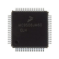
MC9S08JM60CLH Freescale, MC9S08JM60CLH Datasheet - Page 335

MC9S08JM60CLH
Manufacturer Part Number
MC9S08JM60CLH
Description
Manufacturer
Freescale
Datasheet
1.MC9S08JM60CLH.pdf
(388 pages)
Specifications of MC9S08JM60CLH
Cpu Family
HCS08
Device Core Size
8b
Frequency (max)
24MHz
Interface Type
SCI/SPI
Total Internal Ram Size
4KB
# I/os (max)
51
Number Of Timers - General Purpose
8
Operating Supply Voltage (typ)
3.3/5V
Operating Supply Voltage (max)
5.5V
Operating Supply Voltage (min)
2.7V
On-chip Adc
12-chx12-bit
Instruction Set Architecture
CISC
Operating Temp Range
-40C to 85C
Operating Temperature Classification
Industrial
Mounting
Surface Mount
Pin Count
64
Package Type
LQFP
Program Memory Type
Flash
Program Memory Size
60KB
Lead Free Status / RoHS Status
Compliant
Available stocks
Company
Part Number
Manufacturer
Quantity
Price
Company:
Part Number:
MC9S08JM60CLH
Manufacturer:
Freescale Semiconductor
Quantity:
10 000
Part Number:
MC9S08JM60CLH
Manufacturer:
FREESCALE
Quantity:
20 000
Company:
Part Number:
MC9S08JM60CLHE
Manufacturer:
AZBIL
Quantity:
1 000
- Current page: 335 of 388
- Download datasheet (5Mb)
1
Freescale Semiconductor
SYNC
ACK_ENABLE
ACK_DISABLE
BACKGROUND
READ_STATUS
WRITE_CONTROL
READ_BYTE
READ_BYTE_WS
READ_LAST
WRITE_BYTE
WRITE_BYTE_WS
READ_BKPT
WRITE_BKPT
GO
TRACE1
TAGGO
READ_A
READ_CCR
READ_PC
READ_HX
READ_SP
READ_NEXT
READ_NEXT_WS
WRITE_A
WRITE_CCR
WRITE_PC
WRITE_HX
WRITE_SP
WRITE_NEXT
WRITE_NEXT_WS
The SYNC command is a special operation that does not have a command code.
Mnemonic
Command
Non-intrusive
Non-intrusive
Non-intrusive
Non-intrusive
Non-intrusive
Non-intrusive
Non-intrusive
Non-intrusive
Non-intrusive
Non-intrusive
Non-intrusive
Non-intrusive
Non-intrusive
Active BDM
Active BDM
Active BDM
Active BDM
Active BDM
Active BDM
Active BDM
Active BDM
Active BDM
Active BDM
Active BDM
Active BDM
Active BDM
Active BDM
Active BDM
Active BDM
Active BDM
Non-intrusive
Active BDM/
Table 18-1. BDC Command Summary
MC9S08JM60 Series Data Sheet, Rev. 3
n/a
D5/d
D6/d
90/d
E4/SS
C4/CC
E0/AAAA/d/RD
E1/AAAA/d/SS/RD
E8/SS/RD
C0/AAAA/WD/d
C1/AAAA/WD/d/SS
E2/RBKP
C2/WBKP
08/d
10/d
18/d
68/d/RD
69/d/RD
6B/d/RD16
6C/d/RD16
6F/d/RD16
70/d/RD
71/d/SS/RD
48/WD/d
49/WD/d
4B/WD16/d
4C/WD16/d
4F/WD16/d
50/WD/d
51/WD/d/SS
1
Structure
Coding
Request a timed reference pulse to determine
target BDC communication speed
Enable acknowledge protocol. Refer to
Freescale document order no. HCS08RMv1/D.
Disable acknowledge protocol. Refer to
Freescale document order no. HCS08RMv1/D.
Enter active background mode if enabled
(ignore if ENBDM bit equals 0)
Read BDC status from BDCSCR
Write BDC controls in BDCSCR
Read a byte from target memory
Read a byte and report status
Re-read byte from address just read and report
status
Write a byte to target memory
Write a byte and report status
Read BDCBKPT breakpoint register
Write BDCBKPT breakpoint register
Go to execute the user application program
starting at the address currently in the PC
Trace 1 user instruction at the address in the
PC, then return to active background mode
Same as GO but enable external tagging
(HCS08 devices have no external tagging pin)
Read accumulator (A)
Read condition code register (CCR)
Read program counter (PC)
Read H and X register pair (H:X)
Read stack pointer (SP)
Increment H:X by one then read memory byte
located at H:X
Increment H:X by one then read memory byte
located at H:X. Report status and data.
Write accumulator (A)
Write condition code register (CCR)
Write program counter (PC)
Write H and X register pair (H:X)
Write stack pointer (SP)
Increment H:X by one, then write memory byte
located at H:X
Increment H:X by one, then write memory byte
located at H:X. Also report status.
Description
Development Support
335
Related parts for MC9S08JM60CLH
Image
Part Number
Description
Manufacturer
Datasheet
Request
R

Part Number:
Description:
TOWER ELEVATOR BOARDS HARDWARE
Manufacturer:
Freescale Semiconductor
Datasheet:

Part Number:
Description:
TOWER SERIAL I/O HARDWARE
Manufacturer:
Freescale Semiconductor
Datasheet:

Part Number:
Description:
LCD MODULE FOR TWR SYSTEM
Manufacturer:
Freescale Semiconductor
Datasheet:

Part Number:
Description:
DAUGHTER LCD WVGA I.MX51
Manufacturer:
Freescale Semiconductor
Datasheet:

Part Number:
Description:
TOWER SYSTEM BOARD MPC5125
Manufacturer:
Freescale Semiconductor
Datasheet:

Part Number:
Description:
KIT EVALUATION I.MX51
Manufacturer:
Freescale Semiconductor
Datasheet:

Part Number:
Description:
KIT DEVELOPMENT WINCE IMX25
Manufacturer:
Freescale Semiconductor
Datasheet:

Part Number:
Description:
TOWER SYSTEM KIT MPC5125
Manufacturer:
Freescale Semiconductor
Datasheet:

Part Number:
Description:
TOWER SYSTEM BOARD K40X256
Manufacturer:
Freescale Semiconductor
Datasheet:

Part Number:
Description:
TOWER SYSTEM KIT K40X256
Manufacturer:
Freescale Semiconductor
Datasheet:

Part Number:
Description:
Microcontrollers (MCU) MX28 PLATFORM DEV KIT
Manufacturer:
Freescale Semiconductor
Datasheet:

Part Number:
Description:
MCU, MPU & DSP Development Tools IAR KickStart Kit for Kinetis K60
Manufacturer:
Freescale Semiconductor
Datasheet:

Part Number:
Description:
24BIT HDMI MX535/08
Manufacturer:
Freescale Semiconductor
Datasheet:
Part Number:
Description:
Manufacturer:
Freescale Semiconductor, Inc
Datasheet:
Part Number:
Description:
Manufacturer:
Freescale Semiconductor, Inc
Datasheet:


