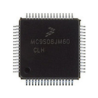
MC9S08JM60CLH Freescale, MC9S08JM60CLH Datasheet - Page 235

MC9S08JM60CLH
Manufacturer Part Number
MC9S08JM60CLH
Description
Manufacturer
Freescale
Datasheet
1.MC9S08JM60CLH.pdf
(388 pages)
Specifications of MC9S08JM60CLH
Cpu Family
HCS08
Device Core Size
8b
Frequency (max)
24MHz
Interface Type
SCI/SPI
Total Internal Ram Size
4KB
# I/os (max)
51
Number Of Timers - General Purpose
8
Operating Supply Voltage (typ)
3.3/5V
Operating Supply Voltage (max)
5.5V
Operating Supply Voltage (min)
2.7V
On-chip Adc
12-chx12-bit
Instruction Set Architecture
CISC
Operating Temp Range
-40C to 85C
Operating Temperature Classification
Industrial
Mounting
Surface Mount
Pin Count
64
Package Type
LQFP
Program Memory Type
Flash
Program Memory Size
60KB
Lead Free Status / RoHS Status
Compliant
Available stocks
Company
Part Number
Manufacturer
Quantity
Price
Company:
Part Number:
MC9S08JM60CLH
Manufacturer:
Freescale Semiconductor
Quantity:
10 000
Part Number:
MC9S08JM60CLH
Manufacturer:
FREESCALE
Quantity:
20 000
Company:
Part Number:
MC9S08JM60CLHE
Manufacturer:
AZBIL
Quantity:
1 000
- Current page: 235 of 388
- Download datasheet (5Mb)
1
14.2.7
This register is actually two separate registers. Reads return the contents of the read-only receive data
buffer and writes go to the write-only transmit data buffer. Reads and writes of this register are also
involved in the automatic flag clearing mechanisms for the SCI status flags.
14.3
The SCI allows full-duplex, asynchronous, NRZ serial communication among the MCU and remote
devices, including other MCUs. The SCI comprises a baud rate generator, transmitter, and receiver block.
The transmitter and receiver operate independently, although they use the same baud rate generator.
During normal operation, the MCU monitors the status of the SCI, writes the data to be transmitted, and
processes received data. The following describes each of the blocks of the SCI.
14.3.1
As shown in
Freescale Semiconductor
Setting TXINV inverts the TxD output for all cases: data bits, start and stop bits, break, and idle.
Reset
TXINV
Field
ORIE
NEIE
FEIE
PEIE
4
3
2
1
0
W
R
1
Functional Description
SCI Data Register (SCIxD)
Baud Rate Generation
Transmit Data Inversion — Setting this bit reverses the polarity of the transmitted data output.
0 Transmit data not inverted
1 Transmit data inverted
Overrun Interrupt Enable — This bit enables the overrun flag (OR) to generate hardware interrupt requests.
0 OR interrupts disabled (use polling).
1 Hardware interrupt requested when OR = 1.
Noise Error Interrupt Enable — This bit enables the noise flag (NF) to generate hardware interrupt requests.
0 NF interrupts disabled (use polling).
1 Hardware interrupt requested when NF = 1.
Framing Error Interrupt Enable — This bit enables the framing error flag (FE) to generate hardware interrupt
requests.
0 FE interrupts disabled (use polling).
1 Hardware interrupt requested when FE = 1.
Parity Error Interrupt Enable — This bit enables the parity error flag (PF) to generate hardware interrupt
requests.
0 PF interrupts disabled (use polling).
1 Hardware interrupt requested when PF = 1.
R7
T7
Figure
0
7
14-12, the clock source for the SCI baud rate generator is the bus-rate clock.
R6
T6
0
6
Table 14-7. SCIxC3 Field Descriptions (continued)
Figure 14-11. SCI Data Register (SCIxD)
MC9S08JM60 Series Data Sheet, Rev. 3
R5
T5
0
5
R4
T4
0
4
Description
R3
T3
3
0
Serial Communications Interface (S08SCIV4)
R2
T2
0
2
R1
T1
0
1
R0
T0
0
0
235
Related parts for MC9S08JM60CLH
Image
Part Number
Description
Manufacturer
Datasheet
Request
R

Part Number:
Description:
TOWER ELEVATOR BOARDS HARDWARE
Manufacturer:
Freescale Semiconductor
Datasheet:

Part Number:
Description:
TOWER SERIAL I/O HARDWARE
Manufacturer:
Freescale Semiconductor
Datasheet:

Part Number:
Description:
LCD MODULE FOR TWR SYSTEM
Manufacturer:
Freescale Semiconductor
Datasheet:

Part Number:
Description:
DAUGHTER LCD WVGA I.MX51
Manufacturer:
Freescale Semiconductor
Datasheet:

Part Number:
Description:
TOWER SYSTEM BOARD MPC5125
Manufacturer:
Freescale Semiconductor
Datasheet:

Part Number:
Description:
KIT EVALUATION I.MX51
Manufacturer:
Freescale Semiconductor
Datasheet:

Part Number:
Description:
KIT DEVELOPMENT WINCE IMX25
Manufacturer:
Freescale Semiconductor
Datasheet:

Part Number:
Description:
TOWER SYSTEM KIT MPC5125
Manufacturer:
Freescale Semiconductor
Datasheet:

Part Number:
Description:
TOWER SYSTEM BOARD K40X256
Manufacturer:
Freescale Semiconductor
Datasheet:

Part Number:
Description:
TOWER SYSTEM KIT K40X256
Manufacturer:
Freescale Semiconductor
Datasheet:

Part Number:
Description:
Microcontrollers (MCU) MX28 PLATFORM DEV KIT
Manufacturer:
Freescale Semiconductor
Datasheet:

Part Number:
Description:
MCU, MPU & DSP Development Tools IAR KickStart Kit for Kinetis K60
Manufacturer:
Freescale Semiconductor
Datasheet:

Part Number:
Description:
24BIT HDMI MX535/08
Manufacturer:
Freescale Semiconductor
Datasheet:
Part Number:
Description:
Manufacturer:
Freescale Semiconductor, Inc
Datasheet:
Part Number:
Description:
Manufacturer:
Freescale Semiconductor, Inc
Datasheet:


