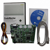
DEMO9S12XEP100 Freescale Semiconductor, DEMO9S12XEP100 Datasheet - Page 117

DEMO9S12XEP100
Manufacturer Part Number
DEMO9S12XEP100
Description
BOARD DEMO FOR MC9S12XEP100
Manufacturer
Freescale Semiconductor
Type
MCUr
Datasheet
1.EVB9S12XEP100.pdf
(1328 pages)
Specifications of DEMO9S12XEP100
Contents
Board, Cables, CD
Processor To Be Evaluated
MC9S12XEP100
Data Bus Width
16 bit
Interface Type
RS-232
Silicon Manufacturer
Freescale
Core Architecture
S12
Core Sub-architecture
S12
Silicon Core Number
MC9S12
Silicon Family Name
S12XE
Rohs Compliant
Yes
For Use With/related Products
MC9S12XEP100
Lead Free Status / RoHS Status
Lead free / RoHS Compliant
Available stocks
Company
Part Number
Manufacturer
Quantity
Price
Company:
Part Number:
DEMO9S12XEP100
Manufacturer:
PANASONIC
Quantity:
46 000
Company:
Part Number:
DEMO9S12XEP100
Manufacturer:
Freescale Semiconductor
Quantity:
135
- Current page: 117 of 1328
- Download datasheet (9Mb)
1. Read: Anytime. In emulation modes, read operations will return the data from the external bus, in all other modes the data source
2. These registers are reset to zero. Two bus clock cycles after reset release the register values are updated with the associated
2.3.11
Freescale Semiconductor
Function
Address 0x0008 (PRR)
is depending on the data direction value.
Write: Anytime. In emulation modes, write operations will also be directed to the external bus.
pin values.
Altern.
Field
Reset
7-2
PE
PE
PE
1
0
W
R
Port E general purpose input/output data—Data Register
Port E bits 7 through 0 are associated with external bus control signals and interrupt inputs. These include mode
select (MODB, MODA), E clock, double frequency E clock, Instruction Tagging High and Low (TAGHI, TAGLO),
Read/Write (RW), Read Enable and Write Enable (RE, WE), Lower Data Select (LDS).
When not used with the alternative functions, Port E pins 7-2 can be used as general purpose I/O.
If the associated data direction bits of these pins are set to 1, a read returns the value of the port register, otherwise
the buffered pin input state is read.
Pins 6 and 5 are inputs with enabled pull-down devices while RESET pin is low.
Pins 7 and 3 are inputs with enabled pull-up devices while RESET pin is low.
Port E general purpose input data and interrupt—Data Register, IRQ input.
This pin can be used as general purpose and IRQ input.
Port E general purpose input data and interrupt—Data Register, XIRQ input.
This pin can be used as general purpose and XIRQ input.
ECLKX2
XCLKS
Port E Data Register (PORTE)
PE7
or
0
7
= Unimplemented or Reserved
TAGHI
MODB
PE6
or
0
6
Table 2-12. PORTE Register Field Descriptions
MC9S12XE-Family Reference Manual , Rev. 1.23
Figure 2-9. Port E Data Register (PORTE)
TAGLO
MODA
PE5
RE
or
or
0
5
ECLK
PE4
0
4
Description
EROMCTL
LSTRB
PE3
LDS
or
or
3
0
Chapter 2 Port Integration Module (S12XEPIMV1)
PE2
RW
WE
or
0
2
Access: User read/write
—
PE1
IRQ
1
(2)
XIRQ
PE0
—
0
2
117
(1)
Related parts for DEMO9S12XEP100
Image
Part Number
Description
Manufacturer
Datasheet
Request
R
Part Number:
Description:
Manufacturer:
Freescale Semiconductor, Inc
Datasheet:
Part Number:
Description:
Manufacturer:
Freescale Semiconductor, Inc
Datasheet:
Part Number:
Description:
Manufacturer:
Freescale Semiconductor, Inc
Datasheet:
Part Number:
Description:
Manufacturer:
Freescale Semiconductor, Inc
Datasheet:
Part Number:
Description:
Manufacturer:
Freescale Semiconductor, Inc
Datasheet:
Part Number:
Description:
Manufacturer:
Freescale Semiconductor, Inc
Datasheet:
Part Number:
Description:
Manufacturer:
Freescale Semiconductor, Inc
Datasheet:
Part Number:
Description:
Manufacturer:
Freescale Semiconductor, Inc
Datasheet:
Part Number:
Description:
Manufacturer:
Freescale Semiconductor, Inc
Datasheet:
Part Number:
Description:
Manufacturer:
Freescale Semiconductor, Inc
Datasheet:
Part Number:
Description:
Manufacturer:
Freescale Semiconductor, Inc
Datasheet:
Part Number:
Description:
Manufacturer:
Freescale Semiconductor, Inc
Datasheet:
Part Number:
Description:
Manufacturer:
Freescale Semiconductor, Inc
Datasheet:
Part Number:
Description:
Manufacturer:
Freescale Semiconductor, Inc
Datasheet:
Part Number:
Description:
Manufacturer:
Freescale Semiconductor, Inc
Datasheet:


