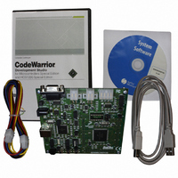
DEMO9S12XEP100 Freescale Semiconductor, DEMO9S12XEP100 Datasheet - Page 599

DEMO9S12XEP100
Manufacturer Part Number
DEMO9S12XEP100
Description
BOARD DEMO FOR MC9S12XEP100
Manufacturer
Freescale Semiconductor
Type
MCUr
Datasheet
1.EVB9S12XEP100.pdf
(1328 pages)
Specifications of DEMO9S12XEP100
Contents
Board, Cables, CD
Processor To Be Evaluated
MC9S12XEP100
Data Bus Width
16 bit
Interface Type
RS-232
Silicon Manufacturer
Freescale
Core Architecture
S12
Core Sub-architecture
S12
Silicon Core Number
MC9S12
Silicon Family Name
S12XE
Rohs Compliant
Yes
For Use With/related Products
MC9S12XEP100
Lead Free Status / RoHS Status
Lead free / RoHS Compliant
Available stocks
Company
Part Number
Manufacturer
Quantity
Price
Company:
Part Number:
DEMO9S12XEP100
Manufacturer:
PANASONIC
Quantity:
46 000
Company:
Part Number:
DEMO9S12XEP100
Manufacturer:
Freescale Semiconductor
Quantity:
135
- Current page: 599 of 1328
- Download datasheet (9Mb)
15.4.1.8
The clock synchronization mechanism can be used as a handshake in data transfer. Slave devices may hold
the SCL low after completion of one byte transfer (9 bits). In such case, it halts the bus clock and forces
the master clock into wait states until the slave releases the SCL line.
15.4.1.9
The clock synchronization mechanism can be used by slaves to slow down the bit rate of a transfer. After
the master has driven SCL low the slave can drive SCL low for the required period and then release it.If
the slave SCL low period is greater than the master SCL low period then the resulting SCL bus signal low
period is stretched.
15.4.1.10 Ten-bit Address
A ten-bit address is indicated if the first 5 bits of the first address byte are 0x11110. The following rules
apply to the first address byte.
The address type is identified by ADTYPE. When ADTYPE is 0, 7-bit address is applied. Reversely, the
address is 10-bit address.Generally, there are two cases of 10-bit address.See the Fig.1-14 and 1-15.
In the figure 1-15,the first two bytes are the similar to figure1-14.After the repeated START(Sr),the first
slave address is transmitted again, but the R/W is 1, meaning that the slave is acted as a transmitter.
15.4.1.11 General Call Address
To broadcast using a general call, a device must first generate the general call address($00), then after
receiving acknowledge, it must transmit data.
In communication, as a slave device, provided the GCEN is asserted, a device acknowledges the broadcast
and receives data until the GCEN is disabled or the master device releases the bus or generates a new
Freescale Semiconductor
S
Because of an order from the United States International Trade Commission, BGA-packaged product lines and partnumbers
indicated here currently are not available from Freescale for import or sale in the United States prior to September 2010
11110+ADR10+ADR9
Slave Add1st 7bits
Figure 15-13. A master-transmitter addresses a slave-receiver with a 10-bit address
Figure 15-14. A master-receiver addresses a slave-transmitter with a 10-bit address
Handshaking
Clock Stretching
S
ADDRESS
11110+ADR10+ADR9
11111XX
11110XX
0000000
0000010
0000011
SLAVE
Slave Add1st 7bits
R/W
0
Table 15-11. Definition of Bits in the First Byte
A1
MC9S12XE-Family Reference Manual Rev. 1.23
Slave Add 2nd byte
ADR[8:1]
R/W
R/W BIT
0
0
x
x
x
x
A1
A2
Slave Add 2nd byte
Chapter 15 Inter-Integrated Circuit (IICV3) Block Description
ADR[8:1]
Sr
Reserved for different bus format
Reserved for future purposes
Reserved for future purposes
11110+ADR10+ADR9
10-bit slave addressing
Slave Add 1st 7bits
General call address
DESCRIPTION
A2
Data
R/W
1
A3
A3
Data
A4
599
Related parts for DEMO9S12XEP100
Image
Part Number
Description
Manufacturer
Datasheet
Request
R
Part Number:
Description:
Manufacturer:
Freescale Semiconductor, Inc
Datasheet:
Part Number:
Description:
Manufacturer:
Freescale Semiconductor, Inc
Datasheet:
Part Number:
Description:
Manufacturer:
Freescale Semiconductor, Inc
Datasheet:
Part Number:
Description:
Manufacturer:
Freescale Semiconductor, Inc
Datasheet:
Part Number:
Description:
Manufacturer:
Freescale Semiconductor, Inc
Datasheet:
Part Number:
Description:
Manufacturer:
Freescale Semiconductor, Inc
Datasheet:
Part Number:
Description:
Manufacturer:
Freescale Semiconductor, Inc
Datasheet:
Part Number:
Description:
Manufacturer:
Freescale Semiconductor, Inc
Datasheet:
Part Number:
Description:
Manufacturer:
Freescale Semiconductor, Inc
Datasheet:
Part Number:
Description:
Manufacturer:
Freescale Semiconductor, Inc
Datasheet:
Part Number:
Description:
Manufacturer:
Freescale Semiconductor, Inc
Datasheet:
Part Number:
Description:
Manufacturer:
Freescale Semiconductor, Inc
Datasheet:
Part Number:
Description:
Manufacturer:
Freescale Semiconductor, Inc
Datasheet:
Part Number:
Description:
Manufacturer:
Freescale Semiconductor, Inc
Datasheet:
Part Number:
Description:
Manufacturer:
Freescale Semiconductor, Inc
Datasheet:


