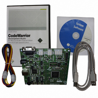
DEMO9S12XEP100 Freescale Semiconductor, DEMO9S12XEP100 Datasheet - Page 783

DEMO9S12XEP100
Manufacturer Part Number
DEMO9S12XEP100
Description
BOARD DEMO FOR MC9S12XEP100
Manufacturer
Freescale Semiconductor
Type
MCUr
Datasheet
1.EVB9S12XEP100.pdf
(1328 pages)
Specifications of DEMO9S12XEP100
Contents
Board, Cables, CD
Processor To Be Evaluated
MC9S12XEP100
Data Bus Width
16 bit
Interface Type
RS-232
Silicon Manufacturer
Freescale
Core Architecture
S12
Core Sub-architecture
S12
Silicon Core Number
MC9S12
Silicon Family Name
S12XE
Rohs Compliant
Yes
For Use With/related Products
MC9S12XEP100
Lead Free Status / RoHS Status
Lead free / RoHS Compliant
Available stocks
Company
Part Number
Manufacturer
Quantity
Price
Company:
Part Number:
DEMO9S12XEP100
Manufacturer:
PANASONIC
Quantity:
46 000
Company:
Part Number:
DEMO9S12XEP100
Manufacturer:
Freescale Semiconductor
Quantity:
135
- Current page: 783 of 1328
- Download datasheet (9Mb)
The SS line can remain active low between successive transfers (can be tied low at all times). This format
is sometimes preferred in systems having a single fixed master and a single slave that drive the MISO data
line.
The SPI interrupt request flag (SPIF) is common to both the master and slave modes. SPIF gets set one
half SCK cycle after the last SCK edge.
21.4.4
Baud rate generation consists of a series of divider stages. Six bits in the SPI baud rate register (SPPR2,
SPPR1, SPPR0, SPR2, SPR1, and SPR0) determine the divisor to the SPI module clock which results in
the SPI baud rate.
The SPI clock rate is determined by the product of the value in the baud rate preselection bits
(SPPR2–SPPR0) and the value in the baud rate selection bits (SPR2–SPR0). The module clock divisor
equation is shown in
Freescale Semiconductor
Because of an order from the United States International Trade Commission, BGA-packaged product lines and partnumbers
indicated here currently are not available from Freescale for import or sale in the United States prior to September 2010
•
End of Idle State
SCK Edge Number
SCK (CPOL = 0)
SCK (CPOL = 1)
SAMPLE I
MOSI/MISO
CHANGE O
CHANGE O
SEL SS (O)
Master only
SEL SS (I)
t
t
t
Figure 21-15. SPI Clock Format 1 (CPHA = 1), with 16-Bit Transfer Width selected (XFRW = 1)
MOSI pin
MISO pin
L
T
I
Back-to-back transfers in master mode
In master mode, if a transmission has completed and new data is available in the SPI data register,
this data is sent out immediately without a trailing and minimum idle time.
MSB first (LSBFE = 0)
LSB first (LSBFE = 1)
= Minimum idling time between transfers (minimum SS high time), not required for back-to-back transfers
= Minimum leading time before the first SCK edge, not required for back-to-back transfers
= Minimum trailing time after the last SCK edge
SPI Baud Rate Generation
Equation
t
L
1
MSB
LSB
2
BaudRateDivisor = (SPPR + 1) • 2
3
Bit 14
Bit 1
4
21-3.
MC9S12XE-Family Reference Manual Rev. 1.23
5
Bit 13
Begin
Bit 2
6
7
Bit 12
Bit 3
8
9
Bit 11
Bit 4
10
11
Bit 10 Bit 9 Bit 8 Bit 7 Bit 6
Bit 5
12
13
Bit 6
14
Transfer
15
Bit 7 Bit 8 Bit 9 Bit 10Bit 11Bit 12Bit 13Bit 14
16
17
18
19
20
(SPR + 1)
21
Bit 5
22
23
Chapter 21 Serial Peripheral Interface (S12SPIV5)
Bit 4 Bit 3 Bit 2 Bit 1
24
25
End
26
27
28
29
30
31
MSB
LSB
32
t
T
Begin of Idle State
t
I
Minimum 1/2 SCK
for t
t
L
T
, t
l
, t
L
Eqn. 21-3
783
Related parts for DEMO9S12XEP100
Image
Part Number
Description
Manufacturer
Datasheet
Request
R
Part Number:
Description:
Manufacturer:
Freescale Semiconductor, Inc
Datasheet:
Part Number:
Description:
Manufacturer:
Freescale Semiconductor, Inc
Datasheet:
Part Number:
Description:
Manufacturer:
Freescale Semiconductor, Inc
Datasheet:
Part Number:
Description:
Manufacturer:
Freescale Semiconductor, Inc
Datasheet:
Part Number:
Description:
Manufacturer:
Freescale Semiconductor, Inc
Datasheet:
Part Number:
Description:
Manufacturer:
Freescale Semiconductor, Inc
Datasheet:
Part Number:
Description:
Manufacturer:
Freescale Semiconductor, Inc
Datasheet:
Part Number:
Description:
Manufacturer:
Freescale Semiconductor, Inc
Datasheet:
Part Number:
Description:
Manufacturer:
Freescale Semiconductor, Inc
Datasheet:
Part Number:
Description:
Manufacturer:
Freescale Semiconductor, Inc
Datasheet:
Part Number:
Description:
Manufacturer:
Freescale Semiconductor, Inc
Datasheet:
Part Number:
Description:
Manufacturer:
Freescale Semiconductor, Inc
Datasheet:
Part Number:
Description:
Manufacturer:
Freescale Semiconductor, Inc
Datasheet:
Part Number:
Description:
Manufacturer:
Freescale Semiconductor, Inc
Datasheet:
Part Number:
Description:
Manufacturer:
Freescale Semiconductor, Inc
Datasheet:


