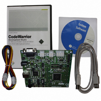
DEMO9S12XEP100 Freescale Semiconductor, DEMO9S12XEP100 Datasheet - Page 650

DEMO9S12XEP100
Manufacturer Part Number
DEMO9S12XEP100
Description
BOARD DEMO FOR MC9S12XEP100
Manufacturer
Freescale Semiconductor
Type
MCUr
Datasheet
1.EVB9S12XEP100.pdf
(1328 pages)
Specifications of DEMO9S12XEP100
Contents
Board, Cables, CD
Processor To Be Evaluated
MC9S12XEP100
Data Bus Width
16 bit
Interface Type
RS-232
Silicon Manufacturer
Freescale
Core Architecture
S12
Core Sub-architecture
S12
Silicon Core Number
MC9S12
Silicon Family Name
S12XE
Rohs Compliant
Yes
For Use With/related Products
MC9S12XEP100
Lead Free Status / RoHS Status
Lead free / RoHS Compliant
Available stocks
Company
Part Number
Manufacturer
Quantity
Price
Company:
Part Number:
DEMO9S12XEP100
Manufacturer:
PANASONIC
Quantity:
46 000
Company:
Part Number:
DEMO9S12XEP100
Manufacturer:
Freescale Semiconductor
Quantity:
135
- Current page: 650 of 1328
- Download datasheet (9Mb)
Chapter 16 Freescale’s Scalable Controller Area Network (S12MSCANV3)
16.4.3.1
The MSCAN protects the user from accidentally violating the CAN protocol through programming errors.
The protection logic implements the following features:
16.4.3.2
Figure 16-43
The clock source bit (CLKSRC) in the CANCTL1 register (16.3.2.2/16-615) defines whether the internal
CANCLK is connected to the output of a crystal oscillator (oscillator clock) or to the bus clock.
The clock source has to be chosen such that the tight oscillator tolerance requirements (up to 0.4%) of the
CAN protocol are met. Additionally, for high CAN bus rates (1 Mbps), a 45% to 55% duty cycle of the
clock is required.
If the bus clock is generated from a PLL, it is recommended to select the oscillator clock rather than the
bus clock due to jitter considerations, especially at the faster CAN bus rates.
650
•
•
•
•
The receive and transmit error counters cannot be written or otherwise manipulated.
All registers which control the configuration of the MSCAN cannot be modified while the MSCAN
is on-line. The MSCAN has to be in Initialization Mode. The corresponding INITRQ/INITAK
handshake bits in the CANCTL0/CANCTL1 registers (see
Register 0
— MSCAN control 1 register (CANCTL1)
— MSCAN bus timing registers 0 and 1 (CANBTR0, CANBTR1)
— MSCAN identifier acceptance control register (CANIDAC)
— MSCAN identifier acceptance registers (CANIDAR0–CANIDAR7)
— MSCAN identifier mask registers (CANIDMR0–CANIDMR7)
The TXCAN is immediately forced to a recessive state when the MSCAN goes into the power
down mode or initialization mode (see
Section 16.4.4.5, “MSCAN Initialization
The MSCAN enable bit (CANE) is writable only once in normal system operation modes, which
provides further protection against inadvertently disabling the MSCAN.
Oscillator Clock
Bus Clock
Protocol Violation Protection
Clock System
shows the structure of the MSCAN clock generation circuitry.
(CANCTL0)”) serve as a lock to protect the following registers:
MC9S12XE-Family Reference Manual , Rev. 1.23
Figure 16-43. MSCAN Clocking Scheme
CLKSRC
Section 16.4.5.6, “MSCAN Power Down
Mode”).
CANCLK
MSCAN
CLKSRC
Prescaler
(1 .. 64)
Section 16.3.2.1, “MSCAN Control
Time quanta clock (Tq)
Freescale Semiconductor
Mode,” and
Related parts for DEMO9S12XEP100
Image
Part Number
Description
Manufacturer
Datasheet
Request
R
Part Number:
Description:
Manufacturer:
Freescale Semiconductor, Inc
Datasheet:
Part Number:
Description:
Manufacturer:
Freescale Semiconductor, Inc
Datasheet:
Part Number:
Description:
Manufacturer:
Freescale Semiconductor, Inc
Datasheet:
Part Number:
Description:
Manufacturer:
Freescale Semiconductor, Inc
Datasheet:
Part Number:
Description:
Manufacturer:
Freescale Semiconductor, Inc
Datasheet:
Part Number:
Description:
Manufacturer:
Freescale Semiconductor, Inc
Datasheet:
Part Number:
Description:
Manufacturer:
Freescale Semiconductor, Inc
Datasheet:
Part Number:
Description:
Manufacturer:
Freescale Semiconductor, Inc
Datasheet:
Part Number:
Description:
Manufacturer:
Freescale Semiconductor, Inc
Datasheet:
Part Number:
Description:
Manufacturer:
Freescale Semiconductor, Inc
Datasheet:
Part Number:
Description:
Manufacturer:
Freescale Semiconductor, Inc
Datasheet:
Part Number:
Description:
Manufacturer:
Freescale Semiconductor, Inc
Datasheet:
Part Number:
Description:
Manufacturer:
Freescale Semiconductor, Inc
Datasheet:
Part Number:
Description:
Manufacturer:
Freescale Semiconductor, Inc
Datasheet:
Part Number:
Description:
Manufacturer:
Freescale Semiconductor, Inc
Datasheet:


