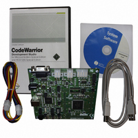
DEMO9S12XEP100 Freescale Semiconductor, DEMO9S12XEP100 Datasheet - Page 1173

DEMO9S12XEP100
Manufacturer Part Number
DEMO9S12XEP100
Description
BOARD DEMO FOR MC9S12XEP100
Manufacturer
Freescale Semiconductor
Type
MCUr
Datasheet
1.EVB9S12XEP100.pdf
(1328 pages)
Specifications of DEMO9S12XEP100
Contents
Board, Cables, CD
Processor To Be Evaluated
MC9S12XEP100
Data Bus Width
16 bit
Interface Type
RS-232
Silicon Manufacturer
Freescale
Core Architecture
S12
Core Sub-architecture
S12
Silicon Core Number
MC9S12
Silicon Family Name
S12XE
Rohs Compliant
Yes
For Use With/related Products
MC9S12XEP100
Lead Free Status / RoHS Status
Lead free / RoHS Compliant
Available stocks
Company
Part Number
Manufacturer
Quantity
Price
Company:
Part Number:
DEMO9S12XEP100
Manufacturer:
PANASONIC
Quantity:
46 000
Company:
Part Number:
DEMO9S12XEP100
Manufacturer:
Freescale Semiconductor
Quantity:
135
- Current page: 1173 of 1328
- Download datasheet (9Mb)
29.4
29.4.1
Flash command operations are used to modify Flash memory contents or configure module resources for
EEE operation.
The next sections describe:
29.4.1.1
Prior to issuing any Flash program or erase command after a reset, the user is required to write the
FCLKDIV register to divide OSCCLK down to a target FCLK of 1 MHz.
values for the FDIV field based on OSCCLK frequency.
When the FCLKDIV register is written, the FDIVLD bit is set automatically. If the FDIVLD bit is 0, the
FCLKDIV register has not been written since the last reset. If the FCLKDIV register has not been written,
any Flash program or erase command loaded during a command write sequence will not execute and the
ACCERR bit in the FSTAT register will set.
29.4.1.2
The Memory Controller will launch all valid Flash commands entered using a command write sequence.
Before launching a command, the ACCERR and FPVIOL bits in the FSTAT register must be clear (see
Section
sequence. If CCIF is 0, the previous command write sequence is still active, a new command write
sequence cannot be started, and all writes to the FCCOB register are ignored.
Freescale Semiconductor
•
•
•
How to write the FCLKDIV register that is used to generate a time base (FCLK) derived from
OSCCLK for Flash program and erase command operations
The command write sequence used to set Flash command parameters and launch execution
Valid Flash commands available for execution
29.3.2.7) and the CCIF flag should be tested to determine the status of the current command write
Functional Description
Flash Command Operations
Writing the FCLKDIV Register
Command Write Sequence
Programming or erasing the Flash memory cannot be performed if the bus
clock runs at less than 1 MHz. Setting FDIV too high can destroy the Flash
memory due to overstress. Setting FDIV too low can result in incomplete
programming or erasure of the Flash memory cells.
Writes to any Flash register must be avoided while a Flash command is
active (CCIF=0) to prevent corruption of Flash register contents and
Memory Controller behavior.
MC9S12XE-Family Reference Manual , Rev. 1.23
CAUTION
NOTE
Chapter 29 1024 KByte Flash Module (S12XFTM1024K5V2)
Table 29-9
shows recommended
1173
Related parts for DEMO9S12XEP100
Image
Part Number
Description
Manufacturer
Datasheet
Request
R
Part Number:
Description:
Manufacturer:
Freescale Semiconductor, Inc
Datasheet:
Part Number:
Description:
Manufacturer:
Freescale Semiconductor, Inc
Datasheet:
Part Number:
Description:
Manufacturer:
Freescale Semiconductor, Inc
Datasheet:
Part Number:
Description:
Manufacturer:
Freescale Semiconductor, Inc
Datasheet:
Part Number:
Description:
Manufacturer:
Freescale Semiconductor, Inc
Datasheet:
Part Number:
Description:
Manufacturer:
Freescale Semiconductor, Inc
Datasheet:
Part Number:
Description:
Manufacturer:
Freescale Semiconductor, Inc
Datasheet:
Part Number:
Description:
Manufacturer:
Freescale Semiconductor, Inc
Datasheet:
Part Number:
Description:
Manufacturer:
Freescale Semiconductor, Inc
Datasheet:
Part Number:
Description:
Manufacturer:
Freescale Semiconductor, Inc
Datasheet:
Part Number:
Description:
Manufacturer:
Freescale Semiconductor, Inc
Datasheet:
Part Number:
Description:
Manufacturer:
Freescale Semiconductor, Inc
Datasheet:
Part Number:
Description:
Manufacturer:
Freescale Semiconductor, Inc
Datasheet:
Part Number:
Description:
Manufacturer:
Freescale Semiconductor, Inc
Datasheet:
Part Number:
Description:
Manufacturer:
Freescale Semiconductor, Inc
Datasheet:


