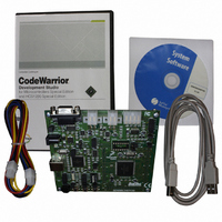
DEMO9S12XEP100 Freescale Semiconductor, DEMO9S12XEP100 Datasheet - Page 1208

DEMO9S12XEP100
Manufacturer Part Number
DEMO9S12XEP100
Description
BOARD DEMO FOR MC9S12XEP100
Manufacturer
Freescale Semiconductor
Type
MCUr
Datasheet
1.EVB9S12XEP100.pdf
(1328 pages)
Specifications of DEMO9S12XEP100
Contents
Board, Cables, CD
Processor To Be Evaluated
MC9S12XEP100
Data Bus Width
16 bit
Interface Type
RS-232
Silicon Manufacturer
Freescale
Core Architecture
S12
Core Sub-architecture
S12
Silicon Core Number
MC9S12
Silicon Family Name
S12XE
Rohs Compliant
Yes
For Use With/related Products
MC9S12XEP100
Lead Free Status / RoHS Status
Lead free / RoHS Compliant
Available stocks
Company
Part Number
Manufacturer
Quantity
Price
Company:
Part Number:
DEMO9S12XEP100
Manufacturer:
PANASONIC
Quantity:
46 000
Company:
Part Number:
DEMO9S12XEP100
Manufacturer:
Freescale Semiconductor
Quantity:
135
- Current page: 1208 of 1328
- Download datasheet (9Mb)
Appendix A Electrical Characteristics
A.1.7
This section describes the operating conditions of the device. Unless otherwise noted those conditions
apply to all the following data.
1
2
3
4
1208
I/O, regulator and analog supply voltage
NVM logic supply voltage
Voltage difference V
Voltage difference V
Voltage difference V
Voltage difference V
Digital logic supply voltage
PLL supply voltage
Oscillator
(Full Swing Pierce)
Bus frequency
C Operating junction temperature range
V Operating junction temperature range
M Operating junction temperature range
The device contains an internal voltage regulator to generate the logic and PLL supply out of the I/O supply. .
This refers to the oscillator base frequency. Typical crystal & resonator tolerances are supported.
Please refer to
Please refer to
ambient temperature T
Operating ambient temperature range
Operating ambient temperature range
Operating ambient temperature range
2
(Loop Controlled Pierce)
Operating Conditions
3
Table A-25
Section A.1.8, “Power Dissipation and Thermal Characteristics”
Please refer to the temperature rating of the device (C, V, M) with regards to
the ambient temperature T
dissipation calculations refer to
Thermal
Using the internal voltage regulator, operation is guaranteed in a power
down until a low voltage reset assertion.
DDX
DDR
SSX
SS1
, V
to V
A
to V
to V
1
and device junction temperature T
1
SS2
Rating
Characteristics”.
SSA
for maximum bus frequency limits with frequency modulation enabled
DDA
DDX
, V
SS3
MC9S12XE-Family Reference Manual , Rev. 1.23
, V
SSPLL
4
2
2
Table A-4. Operating Conditions
to V
A
SSX
and the junction temperature T
Section A.1.8, “Power Dissipation and
NOTE
NOTE
J
.
Symbol
V
∆
∆
V
∆
V
∆
DDPLL
VDDR
V
VDDX
VSSX
f
f
DD35
VSS
T J
T A
T J
T A
T J
T A
DDF
osc
bus
DD
3.13
–0.1
–0.1
1.72
1.72
for more details about the relation between
Min
–40
–40
–40
–40
–40
–40
2.7
0.5
4
2
J
. For power
refer to
refer to
Typ
2.8
1.8
1.8
27
27
27
—
—
—
—
—
—
5
0
0
Table A-15
Table A-15
Freescale Semiconductor
Max
1.98
1.98
110
130
105
150
125
5.5
2.9
0.1
0.1
16
40
50
85
MHz
MHz
Unit
°C
°C
°C
V
V
V
V
V
V
Related parts for DEMO9S12XEP100
Image
Part Number
Description
Manufacturer
Datasheet
Request
R
Part Number:
Description:
Manufacturer:
Freescale Semiconductor, Inc
Datasheet:
Part Number:
Description:
Manufacturer:
Freescale Semiconductor, Inc
Datasheet:
Part Number:
Description:
Manufacturer:
Freescale Semiconductor, Inc
Datasheet:
Part Number:
Description:
Manufacturer:
Freescale Semiconductor, Inc
Datasheet:
Part Number:
Description:
Manufacturer:
Freescale Semiconductor, Inc
Datasheet:
Part Number:
Description:
Manufacturer:
Freescale Semiconductor, Inc
Datasheet:
Part Number:
Description:
Manufacturer:
Freescale Semiconductor, Inc
Datasheet:
Part Number:
Description:
Manufacturer:
Freescale Semiconductor, Inc
Datasheet:
Part Number:
Description:
Manufacturer:
Freescale Semiconductor, Inc
Datasheet:
Part Number:
Description:
Manufacturer:
Freescale Semiconductor, Inc
Datasheet:
Part Number:
Description:
Manufacturer:
Freescale Semiconductor, Inc
Datasheet:
Part Number:
Description:
Manufacturer:
Freescale Semiconductor, Inc
Datasheet:
Part Number:
Description:
Manufacturer:
Freescale Semiconductor, Inc
Datasheet:
Part Number:
Description:
Manufacturer:
Freescale Semiconductor, Inc
Datasheet:
Part Number:
Description:
Manufacturer:
Freescale Semiconductor, Inc
Datasheet:


