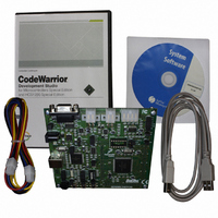
DEMO9S12XEP100 Freescale Semiconductor, DEMO9S12XEP100 Datasheet - Page 777

DEMO9S12XEP100
Manufacturer Part Number
DEMO9S12XEP100
Description
BOARD DEMO FOR MC9S12XEP100
Manufacturer
Freescale Semiconductor
Type
MCUr
Datasheet
1.EVB9S12XEP100.pdf
(1328 pages)
Specifications of DEMO9S12XEP100
Contents
Board, Cables, CD
Processor To Be Evaluated
MC9S12XEP100
Data Bus Width
16 bit
Interface Type
RS-232
Silicon Manufacturer
Freescale
Core Architecture
S12
Core Sub-architecture
S12
Silicon Core Number
MC9S12
Silicon Family Name
S12XE
Rohs Compliant
Yes
For Use With/related Products
MC9S12XEP100
Lead Free Status / RoHS Status
Lead free / RoHS Compliant
Available stocks
Company
Part Number
Manufacturer
Quantity
Price
Company:
Part Number:
DEMO9S12XEP100
Manufacturer:
PANASONIC
Quantity:
46 000
Company:
Part Number:
DEMO9S12XEP100
Manufacturer:
Freescale Semiconductor
Quantity:
135
- Current page: 777 of 1328
- Download datasheet (9Mb)
21.4.2
The SPI operates in slave mode when the MSTR bit in SPI control register 1 is clear.
Freescale Semiconductor
Because of an order from the United States International Trade Commission, BGA-packaged product lines and partnumbers
indicated here currently are not available from Freescale for import or sale in the United States prior to September 2010
•
•
•
drive the MOSI and SCK lines. In this case, the SPI immediately switches to slave mode, by
clearing the MSTR bit and also disables the slave output buffer MISO (or SISO in bidirectional
mode). So the result is that all outputs are disabled and SCK, MOSI, and MISO are inputs. If a
transmission is in progress when the mode fault occurs, the transmission is aborted and the SPI is
forced into idle state.
This mode fault error also sets the mode fault (MODF) flag in the SPI status register (SPISR). If
the SPI interrupt enable bit (SPIE) is set when the MODF flag becomes set, then an SPI interrupt
sequence is also requested.
When a write to the SPI data register in the master occurs, there is a half SCK-cycle delay. After
the delay, SCK is started within the master. The rest of the transfer operation differs slightly,
depending on the clock format specified by the SPI clock phase bit, CPHA, in SPI control register 1
(see
Serial clock
In slave mode, SCK is the SPI clock input from the master.
MISO, MOSI pin
In slave mode, the function of the serial data output pin (MISO) and serial data input pin (MOSI)
is determined by the SPC0 bit and BIDIROE bit in SPI control register 2.
SS pin
The SS pin is the slave select input. Before a data transmission occurs, the SS pin of the slave SPI
must be low. SS must remain low until the transmission is complete. If SS goes high, the SPI is
forced into idle state.
The SS input also controls the serial data output pin, if SS is high (not selected), the serial data
output pin is high impedance, and, if SS is low, the first bit in the SPI data register is driven out of
the serial data output pin. Also, if the slave is not selected (SS is high), then the SCK input is
ignored and no internal shifting of the SPI shift register occurs.
Although the SPI is capable of duplex operation, some SPI peripherals are capable of only
receiving SPI data in a slave mode. For these simpler devices, there is no serial data out pin.
Slave Mode
Section 21.4.3, “Transmission
A change of the bits CPOL, CPHA, SSOE, LSBFE, XFRW, MODFEN,
SPC0, or BIDIROE with SPC0 set, SPPR2-SPPR0 and SPR2-SPR0 in
master mode will abort a transmission in progress and force the SPI into idle
state. The remote slave cannot detect this, therefore the master must ensure
that the remote slave is returned to idle state.
When peripherals with duplex capability are used, take care not to
simultaneously enable two receivers whose serial outputs drive the same
system slave’s serial data output line.
MC9S12XE-Family Reference Manual Rev. 1.23
Formats”).
NOTE
NOTE
Chapter 21 Serial Peripheral Interface (S12SPIV5)
777
Related parts for DEMO9S12XEP100
Image
Part Number
Description
Manufacturer
Datasheet
Request
R
Part Number:
Description:
Manufacturer:
Freescale Semiconductor, Inc
Datasheet:
Part Number:
Description:
Manufacturer:
Freescale Semiconductor, Inc
Datasheet:
Part Number:
Description:
Manufacturer:
Freescale Semiconductor, Inc
Datasheet:
Part Number:
Description:
Manufacturer:
Freescale Semiconductor, Inc
Datasheet:
Part Number:
Description:
Manufacturer:
Freescale Semiconductor, Inc
Datasheet:
Part Number:
Description:
Manufacturer:
Freescale Semiconductor, Inc
Datasheet:
Part Number:
Description:
Manufacturer:
Freescale Semiconductor, Inc
Datasheet:
Part Number:
Description:
Manufacturer:
Freescale Semiconductor, Inc
Datasheet:
Part Number:
Description:
Manufacturer:
Freescale Semiconductor, Inc
Datasheet:
Part Number:
Description:
Manufacturer:
Freescale Semiconductor, Inc
Datasheet:
Part Number:
Description:
Manufacturer:
Freescale Semiconductor, Inc
Datasheet:
Part Number:
Description:
Manufacturer:
Freescale Semiconductor, Inc
Datasheet:
Part Number:
Description:
Manufacturer:
Freescale Semiconductor, Inc
Datasheet:
Part Number:
Description:
Manufacturer:
Freescale Semiconductor, Inc
Datasheet:
Part Number:
Description:
Manufacturer:
Freescale Semiconductor, Inc
Datasheet:


