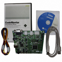
DEMO9S12XEP100 Freescale Semiconductor, DEMO9S12XEP100 Datasheet - Page 739

DEMO9S12XEP100
Manufacturer Part Number
DEMO9S12XEP100
Description
BOARD DEMO FOR MC9S12XEP100
Manufacturer
Freescale Semiconductor
Type
MCUr
Datasheet
1.EVB9S12XEP100.pdf
(1328 pages)
Specifications of DEMO9S12XEP100
Contents
Board, Cables, CD
Processor To Be Evaluated
MC9S12XEP100
Data Bus Width
16 bit
Interface Type
RS-232
Silicon Manufacturer
Freescale
Core Architecture
S12
Core Sub-architecture
S12
Silicon Core Number
MC9S12
Silicon Family Name
S12XE
Rohs Compliant
Yes
For Use With/related Products
MC9S12XEP100
Lead Free Status / RoHS Status
Lead free / RoHS Compliant
Available stocks
Company
Part Number
Manufacturer
Quantity
Price
Company:
Part Number:
DEMO9S12XEP100
Manufacturer:
PANASONIC
Quantity:
46 000
Company:
Part Number:
DEMO9S12XEP100
Manufacturer:
Freescale Semiconductor
Quantity:
135
- Current page: 739 of 1328
- Download datasheet (9Mb)
20.3.2.8
Read: Anytime
Write: Anytime
Freescale Semiconductor
Module Base + 0x0005
Because of an order from the United States International Trade Commission, BGA-packaged product lines and partnumbers
RXPOL
TXPOL
BRK13
Reset
TXDIR
AMAP
indicated here currently are not available from Freescale for import or sale in the United States prior to September 2010
Field
RAF
7
4
3
2
1
0
W
R
AMAP
Alternative Map — This bit controls which registers sharing the same address space are accessible. In the reset
condition the SCI behaves as previous versions. Setting AMAP=1 allows the access to another set of control and
status registers and hides the baud rate and SCI control Register 1.
0 The registers labelled SCIBDH (0x0000),SCIBDL (0x0001), SCICR1 (0x0002) are accessible
1 The registers labelled SCIASR1 (0x0000),SCIACR1 (0x0001), SCIACR2 (0x00002) are accessible
Transmit Polarity — This bit control the polarity of the transmitted data. In NRZ format, a one is represented by
a mark and a zero is represented by a space for normal polarity, and the opposite for inverted polarity. In IrDA
format, a zero is represented by short high pulse in the middle of a bit time remaining idle low for a one for normal
polarity, and a zero is represented by short low pulse in the middle of a bit time remaining idle high for a one for
inverted polarity.
0 Normal polarity
1 Inverted polarity
Receive Polarity — This bit control the polarity of the received data. In NRZ format, a one is represented by a
mark and a zero is represented by a space for normal polarity, and the opposite for inverted polarity. In IrDA
format, a zero is represented by short high pulse in the middle of a bit time remaining idle low for a one for normal
polarity, and a zero is represented by short low pulse in the middle of a bit time remaining idle high for a one for
inverted polarity.
0 Normal polarity
1 Inverted polarity
Break Transmit Character Length — This bit determines whether the transmit break character is 10 or 11 bit
respectively 13 or 14 bits long. The detection of a framing error is not affected by this bit.
0 Break character is 10 or 11 bit long
1 Break character is 13 or 14 bit long
Transmitter Pin Data Direction in Single-Wire Mode — This bit determines whether the TXD pin is going to
be used as an input or output, in the single-wire mode of operation. This bit is only relevant in the single-wire
mode of operation.
0 TXD pin to be used as an input in single-wire mode
1 TXD pin to be used as an output in single-wire mode
Receiver Active Flag — RAF is set when the receiver detects a logic 0 during the RT1 time period of the start
bit search. RAF is cleared when the receiver detects an idle character.
0 No reception in progress
1 Reception in progress
SCI Status Register 2 (SCISR2)
0
7
= Unimplemented or Reserved
0
0
6
Figure 20-11. SCI Status Register 2 (SCISR2)
MC9S12XE-Family Reference Manual Rev. 1.23
Table 20-12. SCISR2 Field Descriptions
5
0
0
TXPOL
0
4
Description
RXPOL
Chapter 20 Serial Communication Interface (S12SCIV5)
0
3
BRK13
2
0
TXDIR
0
1
RAF
0
0
739
Related parts for DEMO9S12XEP100
Image
Part Number
Description
Manufacturer
Datasheet
Request
R
Part Number:
Description:
Manufacturer:
Freescale Semiconductor, Inc
Datasheet:
Part Number:
Description:
Manufacturer:
Freescale Semiconductor, Inc
Datasheet:
Part Number:
Description:
Manufacturer:
Freescale Semiconductor, Inc
Datasheet:
Part Number:
Description:
Manufacturer:
Freescale Semiconductor, Inc
Datasheet:
Part Number:
Description:
Manufacturer:
Freescale Semiconductor, Inc
Datasheet:
Part Number:
Description:
Manufacturer:
Freescale Semiconductor, Inc
Datasheet:
Part Number:
Description:
Manufacturer:
Freescale Semiconductor, Inc
Datasheet:
Part Number:
Description:
Manufacturer:
Freescale Semiconductor, Inc
Datasheet:
Part Number:
Description:
Manufacturer:
Freescale Semiconductor, Inc
Datasheet:
Part Number:
Description:
Manufacturer:
Freescale Semiconductor, Inc
Datasheet:
Part Number:
Description:
Manufacturer:
Freescale Semiconductor, Inc
Datasheet:
Part Number:
Description:
Manufacturer:
Freescale Semiconductor, Inc
Datasheet:
Part Number:
Description:
Manufacturer:
Freescale Semiconductor, Inc
Datasheet:
Part Number:
Description:
Manufacturer:
Freescale Semiconductor, Inc
Datasheet:
Part Number:
Description:
Manufacturer:
Freescale Semiconductor, Inc
Datasheet:


