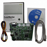
DEMO9S12XEP100 Freescale Semiconductor, DEMO9S12XEP100 Datasheet - Page 64

DEMO9S12XEP100
Manufacturer Part Number
DEMO9S12XEP100
Description
BOARD DEMO FOR MC9S12XEP100
Manufacturer
Freescale Semiconductor
Type
MCUr
Datasheet
1.EVB9S12XEP100.pdf
(1328 pages)
Specifications of DEMO9S12XEP100
Contents
Board, Cables, CD
Processor To Be Evaluated
MC9S12XEP100
Data Bus Width
16 bit
Interface Type
RS-232
Silicon Manufacturer
Freescale
Core Architecture
S12
Core Sub-architecture
S12
Silicon Core Number
MC9S12
Silicon Family Name
S12XE
Rohs Compliant
Yes
For Use With/related Products
MC9S12XEP100
Lead Free Status / RoHS Status
Lead free / RoHS Compliant
Available stocks
Company
Part Number
Manufacturer
Quantity
Price
Company:
Part Number:
DEMO9S12XEP100
Manufacturer:
PANASONIC
Quantity:
46 000
Company:
Part Number:
DEMO9S12XEP100
Manufacturer:
Freescale Semiconductor
Quantity:
135
- Current page: 64 of 1328
- Download datasheet (9Mb)
Chapter 1 Device Overview MC9S12XE-Family
1.2.3.13
PE6 is a general-purpose input or output pin. It is used as a MCU operating mode select pin during reset.
The state of this pin is latched to the MODB bit at the rising edge of RESET. This pin is an input with a
pull-down device which is only active when RESET is low. TAGHI is used to tag the high half of the
instruction word being read into the instruction queue.
The input voltage threshold for PE6 can be configured to reduced levels, to allow data from an external
3.3-V peripheral to be read by the MCU operating at 5.0 V. The input voltage threshold for PE6 is
configured to reduced levels out of reset in expanded and emulation modes.
1.2.3.14
PE5 is a general-purpose input or output pin. It is used as an MCU operating mode select pin during reset.
The state of this pin is latched to the MODA bit at the rising edge of RESET. This pin is shared with the
read enable RE output. This pin is an input with a pull-down device which is only active when RESET is
low. TAGLO is used to tag the low half of the instruction word being read into the instruction queue.
The input voltage threshold for PE5 can be configured to reduced levels, to allow data from an external
3.3-V peripheral to be read by the MCU operating at 5.0 V. The input voltage threshold for PE5 is
configured to reduced levels out of reset in expanded and emulation modes.
1.2.3.15
PE4 is a general-purpose input or output pin. It can be configured to drive the internal bus clock ECLK.
ECLK can be used as a timing reference. The ECLK output has a programmable prescaler.
1.2.3.16
PE3 is a general-purpose input or output pin. In MCU expanded modes of operation, LSTRB or LDS can
be used for the low byte strobe function to indicate the type of bus access. At the rising edge of RESET
the state of this pin is latched to the EROMON bit.
1.2.3.17
PE2 is a general-purpose input or output pin. In MCU expanded modes of operations, this pin drives the
read/write output signal or write enable output signal for the external bus. It indicates the direction of data
on the external bus.
1.2.3.18
PE1 is a general-purpose input pin and the maskable interrupt request input that provides a means of
applying asynchronous interrupt requests. This will wake up the MCU from stop or wait mode.
1.2.3.19
PE0 is a general-purpose input pin and the non-maskable interrupt request input that provides a means of
applying asynchronous interrupt requests. This will wake up the MCU from stop or wait mode. The XIRQ
64
Because of an order from the United States International Trade Commission, BGA-packaged product lines and partnumbers
indicated here currently are not available from Freescale for import or sale in the United States prior to September 2010
PE6 / MODB / TAGHI — Port E I/O Pin 6
PE5 / MODA / TAGLO / RE — Port E I/O Pin 5
PE4 / ECLK — Port E I/O Pin 4
PE3 / LSTRB / LDS / EROMCTL— Port E I/O Pin 3
PE2 / R/W / WE— Port E I/O Pin 2
PE1 / IRQ — Port E Input Pin 1
PE0 / XIRQ — Port E Input Pin 0
MC9S12XE-Family Reference Manual , Rev. 1.23
Freescale Semiconductor
Related parts for DEMO9S12XEP100
Image
Part Number
Description
Manufacturer
Datasheet
Request
R
Part Number:
Description:
Manufacturer:
Freescale Semiconductor, Inc
Datasheet:
Part Number:
Description:
Manufacturer:
Freescale Semiconductor, Inc
Datasheet:
Part Number:
Description:
Manufacturer:
Freescale Semiconductor, Inc
Datasheet:
Part Number:
Description:
Manufacturer:
Freescale Semiconductor, Inc
Datasheet:
Part Number:
Description:
Manufacturer:
Freescale Semiconductor, Inc
Datasheet:
Part Number:
Description:
Manufacturer:
Freescale Semiconductor, Inc
Datasheet:
Part Number:
Description:
Manufacturer:
Freescale Semiconductor, Inc
Datasheet:
Part Number:
Description:
Manufacturer:
Freescale Semiconductor, Inc
Datasheet:
Part Number:
Description:
Manufacturer:
Freescale Semiconductor, Inc
Datasheet:
Part Number:
Description:
Manufacturer:
Freescale Semiconductor, Inc
Datasheet:
Part Number:
Description:
Manufacturer:
Freescale Semiconductor, Inc
Datasheet:
Part Number:
Description:
Manufacturer:
Freescale Semiconductor, Inc
Datasheet:
Part Number:
Description:
Manufacturer:
Freescale Semiconductor, Inc
Datasheet:
Part Number:
Description:
Manufacturer:
Freescale Semiconductor, Inc
Datasheet:
Part Number:
Description:
Manufacturer:
Freescale Semiconductor, Inc
Datasheet:


