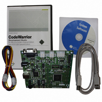
DEMO9S12XEP100 Freescale Semiconductor, DEMO9S12XEP100 Datasheet - Page 929

DEMO9S12XEP100
Manufacturer Part Number
DEMO9S12XEP100
Description
BOARD DEMO FOR MC9S12XEP100
Manufacturer
Freescale Semiconductor
Type
MCUr
Datasheet
1.EVB9S12XEP100.pdf
(1328 pages)
Specifications of DEMO9S12XEP100
Contents
Board, Cables, CD
Processor To Be Evaluated
MC9S12XEP100
Data Bus Width
16 bit
Interface Type
RS-232
Silicon Manufacturer
Freescale
Core Architecture
S12
Core Sub-architecture
S12
Silicon Core Number
MC9S12
Silicon Family Name
S12XE
Rohs Compliant
Yes
For Use With/related Products
MC9S12XEP100
Lead Free Status / RoHS Status
Lead free / RoHS Compliant
Available stocks
Company
Part Number
Manufacturer
Quantity
Price
Company:
Part Number:
DEMO9S12XEP100
Manufacturer:
PANASONIC
Quantity:
46 000
Company:
Part Number:
DEMO9S12XEP100
Manufacturer:
Freescale Semiconductor
Quantity:
135
- Current page: 929 of 1328
- Download datasheet (9Mb)
25.4.2
This section provides details of all available Flash commands launched by a command write sequence. The
ACCERR bit in the FSTAT register will be set during the command write sequence if any of the following
illegal steps are performed, causing the command not to be processed by the Memory Controller:
If a Flash block is read during execution of an algorithm (CCIF = 0) on that same block, the read operation
will return invalid data. If the SFDIF or DFDIF flags were not previously set when the invalid read
operation occurred, both the SFDIF and DFDIF flags will be set and the FECCR registers will be loaded
with the global address used in the invalid read operation with the data and parity fields set to all 0.
If the ACCERR or FPVIOL bits are set in the FSTAT register, the user must clear these bits before starting
any command write sequence (see
Freescale Semiconductor
FCMD
0x0D
•
•
•
0x0B
0x0E
0x0F
0x08
0x10
0x11
0x12
0x13
0x14
0x15
0x20
Starting any command write sequence that programs or erases Flash memory before initializing the
FCLKDIV register
Writing an invalid command as part of the command write sequence
For additional possible errors, refer to the error handling table provided for each command
Flash Command Description
Disable EEPROM
Program D-Flash
Enable EEPROM
Emulation Query
Partition D-Flash
Erase All Blocks
Set User Margin
Set Field Margin
Unsecure Flash
Full Partition D-
Erase Verify D-
Erase D-Flash
Flash Section
Command
Emulation
Emulation
EEPROM
Sector
Flash
Level
Level
Erase all D-Flash (and P-Flash) blocks.
An erase of all Flash blocks is only possible when the FPLDIS, FPHDIS, and FPOPEN
bits in the FPROT register and the EPDIS and EPOPEN bits in the EPROT register are
set prior to launching the command.
Supports a method of releasing MCU security by erasing all D-Flash (and P-Flash) blocks
and verifying that all D-Flash (and P-Flash) blocks are erased.
Specifies a user margin read level for the D-Flash block.
Specifies a field margin read level for the D-Flash block (special modes only).
Erase the D-Flash block and partition an area of the D-Flash block for user access.
Verify that a given number of words starting at the address provided are erased.
Program up to four words in the D-Flash block.
Erase all bytes in a sector of the D-Flash block.
Enable EEPROM emulation where writes to the buffer RAM EEE partition will be copied
to the D-Flash EEE partition.
Suspend all current erase and program activity related to EEPROM emulation but leave
current EEE tags set.
Returns EEE partition and status variables.
Partition an area of the D-Flash block for user access.
MC9S12XE-Family Reference Manual , Rev. 1.23
Section
Table 25-32. D-Flash Commands
25.3.2.7).
Function on D-Flash Memory
Chapter 25 256 KByte Flash Module (S12XFTM256K2V1)
929
Related parts for DEMO9S12XEP100
Image
Part Number
Description
Manufacturer
Datasheet
Request
R
Part Number:
Description:
Manufacturer:
Freescale Semiconductor, Inc
Datasheet:
Part Number:
Description:
Manufacturer:
Freescale Semiconductor, Inc
Datasheet:
Part Number:
Description:
Manufacturer:
Freescale Semiconductor, Inc
Datasheet:
Part Number:
Description:
Manufacturer:
Freescale Semiconductor, Inc
Datasheet:
Part Number:
Description:
Manufacturer:
Freescale Semiconductor, Inc
Datasheet:
Part Number:
Description:
Manufacturer:
Freescale Semiconductor, Inc
Datasheet:
Part Number:
Description:
Manufacturer:
Freescale Semiconductor, Inc
Datasheet:
Part Number:
Description:
Manufacturer:
Freescale Semiconductor, Inc
Datasheet:
Part Number:
Description:
Manufacturer:
Freescale Semiconductor, Inc
Datasheet:
Part Number:
Description:
Manufacturer:
Freescale Semiconductor, Inc
Datasheet:
Part Number:
Description:
Manufacturer:
Freescale Semiconductor, Inc
Datasheet:
Part Number:
Description:
Manufacturer:
Freescale Semiconductor, Inc
Datasheet:
Part Number:
Description:
Manufacturer:
Freescale Semiconductor, Inc
Datasheet:
Part Number:
Description:
Manufacturer:
Freescale Semiconductor, Inc
Datasheet:
Part Number:
Description:
Manufacturer:
Freescale Semiconductor, Inc
Datasheet:


