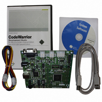
DEMO9S12XEP100 Freescale Semiconductor, DEMO9S12XEP100 Datasheet - Page 201

DEMO9S12XEP100
Manufacturer Part Number
DEMO9S12XEP100
Description
BOARD DEMO FOR MC9S12XEP100
Manufacturer
Freescale Semiconductor
Type
MCUr
Datasheet
1.EVB9S12XEP100.pdf
(1328 pages)
Specifications of DEMO9S12XEP100
Contents
Board, Cables, CD
Processor To Be Evaluated
MC9S12XEP100
Data Bus Width
16 bit
Interface Type
RS-232
Silicon Manufacturer
Freescale
Core Architecture
S12
Core Sub-architecture
S12
Silicon Core Number
MC9S12
Silicon Family Name
S12XE
Rohs Compliant
Yes
For Use With/related Products
MC9S12XEP100
Lead Free Status / RoHS Status
Lead free / RoHS Compliant
Available stocks
Company
Part Number
Manufacturer
Quantity
Price
Company:
Part Number:
DEMO9S12XEP100
Manufacturer:
PANASONIC
Quantity:
46 000
Company:
Part Number:
DEMO9S12XEP100
Manufacturer:
Freescale Semiconductor
Quantity:
135
- Current page: 201 of 1328
- Download datasheet (9Mb)
3.3.2.3
Read: Anytime
Write: Anytime
The global page index register is used to construct a 23 bit address in the global map format. It is only used
when the CPU is executing a global instruction (GLDAA, GLDAB, GLDD, GLDS, GLDX,
GLDY,GSTAA, GSTAB, GSTD, GSTS, GSTX, GSTY) (see CPU Block Guide). The generated global
address is the result of concatenation of the CPU local address [15:0] with the GPAGE register [22:16] (see
Figure
Freescale Semiconductor
Address: 0x0010
Because of an order from the United States International Trade Commission, BGA-packaged product lines and partnumbers
GP[6:0]
Reset
indicated here currently are not available from Freescale for import or sale in the United States prior to September 2010
Field
6–0
W
R
3-7).
Bit22
LDX
MOVB
GLDAA
Global Page Index Bits 6–0 — These page index bits are used to select which of the 128 64-kilobyte pages is
to be accessed.
Global Page Index Register (GPAGE)
0
0
7
XGATE write access to this register during an CPU access which makes use
of this register could lead to unexpected results.
GPAGE Register [6:0]
Example 3-1. This example demonstrates usage of the GPAGE register
#0x5000
#0x14, GPAGE
X
= Unimplemented or Reserved
GP6
0
6
Figure 3-6. Global Page Index Register (GPAGE)
MC9S12XE-Family Reference Manual Rev. 1.23
Figure 3-7. GPAGE Address Mapping
Table 3-9. GPAGE Field Descriptions
GP5
5
0
;Set GPAGE offset to the value of 0x5000
;Initialize GPAGE register with the value of 0x14
;Load Accu A from the global address 0x14_5000
Global Address [22:0]
Bit16
CAUTION
Bit15
GP4
0
4
Description
GP3
0
3
CPU Address [15:0]
Chapter 3 Memory Mapping Control (S12XMMCV4)
GP2
2
0
GP1
0
1
Bit 0
GP0
0
0
201
Related parts for DEMO9S12XEP100
Image
Part Number
Description
Manufacturer
Datasheet
Request
R
Part Number:
Description:
Manufacturer:
Freescale Semiconductor, Inc
Datasheet:
Part Number:
Description:
Manufacturer:
Freescale Semiconductor, Inc
Datasheet:
Part Number:
Description:
Manufacturer:
Freescale Semiconductor, Inc
Datasheet:
Part Number:
Description:
Manufacturer:
Freescale Semiconductor, Inc
Datasheet:
Part Number:
Description:
Manufacturer:
Freescale Semiconductor, Inc
Datasheet:
Part Number:
Description:
Manufacturer:
Freescale Semiconductor, Inc
Datasheet:
Part Number:
Description:
Manufacturer:
Freescale Semiconductor, Inc
Datasheet:
Part Number:
Description:
Manufacturer:
Freescale Semiconductor, Inc
Datasheet:
Part Number:
Description:
Manufacturer:
Freescale Semiconductor, Inc
Datasheet:
Part Number:
Description:
Manufacturer:
Freescale Semiconductor, Inc
Datasheet:
Part Number:
Description:
Manufacturer:
Freescale Semiconductor, Inc
Datasheet:
Part Number:
Description:
Manufacturer:
Freescale Semiconductor, Inc
Datasheet:
Part Number:
Description:
Manufacturer:
Freescale Semiconductor, Inc
Datasheet:
Part Number:
Description:
Manufacturer:
Freescale Semiconductor, Inc
Datasheet:
Part Number:
Description:
Manufacturer:
Freescale Semiconductor, Inc
Datasheet:


