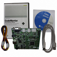
DEMO9S12XEP100 Freescale Semiconductor, DEMO9S12XEP100 Datasheet - Page 806

DEMO9S12XEP100
Manufacturer Part Number
DEMO9S12XEP100
Description
BOARD DEMO FOR MC9S12XEP100
Manufacturer
Freescale Semiconductor
Type
MCUr
Datasheet
1.EVB9S12XEP100.pdf
(1328 pages)
Specifications of DEMO9S12XEP100
Contents
Board, Cables, CD
Processor To Be Evaluated
MC9S12XEP100
Data Bus Width
16 bit
Interface Type
RS-232
Silicon Manufacturer
Freescale
Core Architecture
S12
Core Sub-architecture
S12
Silicon Core Number
MC9S12
Silicon Family Name
S12XE
Rohs Compliant
Yes
For Use With/related Products
MC9S12XEP100
Lead Free Status / RoHS Status
Lead free / RoHS Compliant
Available stocks
Company
Part Number
Manufacturer
Quantity
Price
Company:
Part Number:
DEMO9S12XEP100
Manufacturer:
PANASONIC
Quantity:
46 000
Company:
Part Number:
DEMO9S12XEP100
Manufacturer:
Freescale Semiconductor
Quantity:
135
- Current page: 806 of 1328
- Download datasheet (9Mb)
Module Base + 0x0010 = TC0H
Module Base + 0x0011 = TC0L
Chapter 22 Timer Module (TIM16B8CV2) Block Description
22.3.2.14 Timer Input Capture/Output Compare Registers High and Low 0–7
Depending on the TIOS bit for the corresponding channel, these registers are used to latch the value of the
free-running counter when a defined transition is sensed by the corresponding input capture edge detector
or to trigger an output action for output compare.
Read: Anytime
Write: Anytime for output compare function.Writes to these registers have no meaning or effect during
input capture. All timer input capture/output compare registers are reset to 0x0000.
806
Because of an order from the United States International Trade Commission, BGA-packaged product lines and partnumbers
indicated here currently are not available from Freescale for import or sale in the United States prior to September 2010
Field
TOF
7
Reset
Reset
W
W
R
R
Timer Overflow Flag — Set when 16-bit free-running timer overflows from 0xFFFF to 0x0000. Clearing this bit
requires writing a one to bit 7 of TFLG2 register while the TEN bit of TSCR1 or PAEN bit of PACTL is set to one
(See also TCRE control bit explanation.)
0x0012 = TC1H
0x0014 = TC2H
0x0016 = TC3H
0x0013 = TC1L
0x0015 = TC2L
0x0017 = TC3L
(TCxH and TCxL)
Read/Write access in byte mode for high byte should takes place before low
byte otherwise it will give a different result.
Figure 22-22. Timer Input Capture/Output Compare Register x High (TCxH)
Figure 22-23. Timer Input Capture/Output Compare Register x Low (TCxL)
Bit 15
Bit 7
15
0
0
7
Bit 14
Bit 6
14
0
0
6
MC9S12XE-Family Reference Manual Rev. 1.23
Table 22-17. TRLG2 Field Descriptions
0x0018 = TC4H
0x001A = TC5H
0x001C = TC6H
0x001E = TC7H
0x0019 = TC4L
0x001B = TC5L
0x001D = TC6L
0x001F = TC7L
Bit 13
Bit 5
13
0
0
5
NOTE
Bit 12
Bit 4
12
0
0
4
Description
Bit 11
Bit 3
11
0
0
3
Bit 10
Bit 2
10
0
0
2
Freescale Semiconductor
Bit 9
Bit 1
0
0
9
1
Bit 8
Bit 0
0
0
0
0
Related parts for DEMO9S12XEP100
Image
Part Number
Description
Manufacturer
Datasheet
Request
R
Part Number:
Description:
Manufacturer:
Freescale Semiconductor, Inc
Datasheet:
Part Number:
Description:
Manufacturer:
Freescale Semiconductor, Inc
Datasheet:
Part Number:
Description:
Manufacturer:
Freescale Semiconductor, Inc
Datasheet:
Part Number:
Description:
Manufacturer:
Freescale Semiconductor, Inc
Datasheet:
Part Number:
Description:
Manufacturer:
Freescale Semiconductor, Inc
Datasheet:
Part Number:
Description:
Manufacturer:
Freescale Semiconductor, Inc
Datasheet:
Part Number:
Description:
Manufacturer:
Freescale Semiconductor, Inc
Datasheet:
Part Number:
Description:
Manufacturer:
Freescale Semiconductor, Inc
Datasheet:
Part Number:
Description:
Manufacturer:
Freescale Semiconductor, Inc
Datasheet:
Part Number:
Description:
Manufacturer:
Freescale Semiconductor, Inc
Datasheet:
Part Number:
Description:
Manufacturer:
Freescale Semiconductor, Inc
Datasheet:
Part Number:
Description:
Manufacturer:
Freescale Semiconductor, Inc
Datasheet:
Part Number:
Description:
Manufacturer:
Freescale Semiconductor, Inc
Datasheet:
Part Number:
Description:
Manufacturer:
Freescale Semiconductor, Inc
Datasheet:
Part Number:
Description:
Manufacturer:
Freescale Semiconductor, Inc
Datasheet:


