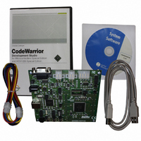
DEMO9S12XEP100 Freescale Semiconductor, DEMO9S12XEP100 Datasheet - Page 758

DEMO9S12XEP100
Manufacturer Part Number
DEMO9S12XEP100
Description
BOARD DEMO FOR MC9S12XEP100
Manufacturer
Freescale Semiconductor
Type
MCUr
Datasheet
1.EVB9S12XEP100.pdf
(1328 pages)
Specifications of DEMO9S12XEP100
Contents
Board, Cables, CD
Processor To Be Evaluated
MC9S12XEP100
Data Bus Width
16 bit
Interface Type
RS-232
Silicon Manufacturer
Freescale
Core Architecture
S12
Core Sub-architecture
S12
Silicon Core Number
MC9S12
Silicon Family Name
S12XE
Rohs Compliant
Yes
For Use With/related Products
MC9S12XEP100
Lead Free Status / RoHS Status
Lead free / RoHS Compliant
Available stocks
Company
Part Number
Manufacturer
Quantity
Price
Company:
Part Number:
DEMO9S12XEP100
Manufacturer:
PANASONIC
Quantity:
46 000
Company:
Part Number:
DEMO9S12XEP100
Manufacturer:
Freescale Semiconductor
Quantity:
135
- Current page: 758 of 1328
- Download datasheet (9Mb)
Chapter 20 Serial Communication Interface (S12SCIV5)
20.4.6.6.1
In this wakeup method, an idle condition on the RXD pin clears the RWU bit and wakes up the SCI. The
initial frame or frames of every message contain addressing information. All receivers evaluate the
addressing information, and receivers for which the message is addressed process the frames that follow.
Any receiver for which a message is not addressed can set its RWU bit and return to the standby state. The
RWU bit remains set and the receiver remains on standby until another idle character appears on the RXD
pin.
Idle line wakeup requires that messages be separated by at least one idle character and that no message
contains idle characters.
The idle character that wakes a receiver does not set the receiver idle bit, IDLE, or the receive data register
full flag, RDRF.
The idle line type bit, ILT, determines whether the receiver begins counting logic 1s as idle character bits
after the start bit or after the stop bit. ILT is in SCI control register 1 (SCICR1).
20.4.6.6.2
In this wakeup method, a logic 1 in the most significant bit (MSB) position of a frame clears the RWU bit
and wakes up the SCI. The logic 1 in the MSB position marks a frame as an address frame that contains
addressing information. All receivers evaluate the addressing information, and the receivers for which the
message is addressed process the frames that follow.Any receiver for which a message is not addressed can
set its RWU bit and return to the standby state. The RWU bit remains set and the receiver remains on
standby until another address frame appears on the RXD pin.
The logic 1 MSB of an address frame clears the receiver’s RWU bit before the stop bit is received and sets
the RDRF flag.
Address mark wakeup allows messages to contain idle characters but requires that the MSB be reserved
for use in address frames.
20.4.7
Normally, the SCI uses two pins for transmitting and receiving. In single-wire operation, the RXD pin is
disconnected from the SCI. The SCI uses the TXD pin for both receiving and transmitting.
758
Because of an order from the United States International Trade Commission, BGA-packaged product lines and partnumbers
indicated here currently are not available from Freescale for import or sale in the United States prior to September 2010
Single-Wire Operation
Idle Input line Wakeup (WAKE = 0)
Address Mark Wakeup (WAKE = 1)
With the WAKE bit clear, setting the RWU bit after the RXD pin has been
idle can cause the receiver to wake up immediately.
Figure 20-30. Single-Wire Operation (LOOPS = 1, RSRC = 1)
Transmitter
MC9S12XE-Family Reference Manual , Rev. 1.23
Receiver
NOTE
RXD
TXD
Freescale Semiconductor
Related parts for DEMO9S12XEP100
Image
Part Number
Description
Manufacturer
Datasheet
Request
R
Part Number:
Description:
Manufacturer:
Freescale Semiconductor, Inc
Datasheet:
Part Number:
Description:
Manufacturer:
Freescale Semiconductor, Inc
Datasheet:
Part Number:
Description:
Manufacturer:
Freescale Semiconductor, Inc
Datasheet:
Part Number:
Description:
Manufacturer:
Freescale Semiconductor, Inc
Datasheet:
Part Number:
Description:
Manufacturer:
Freescale Semiconductor, Inc
Datasheet:
Part Number:
Description:
Manufacturer:
Freescale Semiconductor, Inc
Datasheet:
Part Number:
Description:
Manufacturer:
Freescale Semiconductor, Inc
Datasheet:
Part Number:
Description:
Manufacturer:
Freescale Semiconductor, Inc
Datasheet:
Part Number:
Description:
Manufacturer:
Freescale Semiconductor, Inc
Datasheet:
Part Number:
Description:
Manufacturer:
Freescale Semiconductor, Inc
Datasheet:
Part Number:
Description:
Manufacturer:
Freescale Semiconductor, Inc
Datasheet:
Part Number:
Description:
Manufacturer:
Freescale Semiconductor, Inc
Datasheet:
Part Number:
Description:
Manufacturer:
Freescale Semiconductor, Inc
Datasheet:
Part Number:
Description:
Manufacturer:
Freescale Semiconductor, Inc
Datasheet:
Part Number:
Description:
Manufacturer:
Freescale Semiconductor, Inc
Datasheet:


