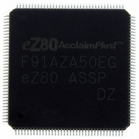
EZ80F91AZA50EG Zilog, EZ80F91AZA50EG Datasheet - Page 107

EZ80F91AZA50EG
Manufacturer Part Number
EZ80F91AZA50EG
Description
IC ACCLAIM MCU 256KB 144LQFP
Manufacturer
Zilog
Series
eZ80® AcclaimPlus!™r
Datasheet
1.EZ80F91AZA50SG.pdf
(387 pages)
Specifications of EZ80F91AZA50EG
Core Processor
Z8
Core Size
8-Bit
Speed
50MHz
Connectivity
Ethernet, I²C, IrDA, SPI, UART/USART
Peripherals
Brown-out Detect/Reset, POR, PWM, WDT
Number Of I /o
32
Program Memory Size
256KB (256K x 8)
Program Memory Type
FLASH
Ram Size
16K x 8
Voltage - Supply (vcc/vdd)
3 V ~ 3.6 V
Oscillator Type
Internal
Operating Temperature
-40°C ~ 105°C
Package / Case
144-LQFP
Processor Series
EZ80F91x
Core
eZ80
Data Bus Width
8 bit
Data Ram Size
16 KB
Interface Type
I2C, IrDA, SPI
Maximum Clock Frequency
50 MHz
Number Of Programmable I/os
32
Number Of Timers
4
Operating Supply Voltage
3 V to 3.6 V
Maximum Operating Temperature
+ 105 C
Mounting Style
SMD/SMT
Development Tools By Supplier
eZ80F910300ZCOG
Minimum Operating Temperature
- 40 C
For Use With
269-4712 - KIT DEV ENCORE 32 SERIES269-4671 - BOARD ZDOTS SBC Z80ACCLAIM PLUS269-4561 - KIT DEV FOR EZ80F91 W/C-COMPILER269-4560 - KIT DEV FOR EZ80F91 W/C-COMPILER
Lead Free Status / RoHS Status
Lead free / RoHS Compliant
Eeprom Size
-
Data Converters
-
Lead Free Status / Rohs Status
Details
Other names
269-4563
Available stocks
Company
Part Number
Manufacturer
Quantity
Price
- Current page: 107 of 387
- Download datasheet (5Mb)
PS027001-0707
Memory Read
Programming Flash Memory
Note:
A memory Read operation uses the address bus and data bus of the eZ80F91 device to
read a single data byte from Flash memory. This Read operation is similar to reads from
RAM. To perform Flash memory reads, the FLASH_CTRL register must be configured to
enable memory access to Flash with the appropriate number of wait states. See
on page 105.
Only the main area of Flash memory is accessible via memory reads. The information
page must be read using I/O access.
I/O Read
A single-byte I/O Read operation uses I/O registers for setting the column, page, and row
address to be read. A Read of the FLASH_DATA register returns the contents of Flash
memory at the designated address. Each access to the FLASH_DATA register causes an
autoincrement of the Flash address stored in the Flash address registers (FLASH_PAGE,
FLASH_ROW, FLASH_COL). To allow for Flash memory access time, the
FLASH_CTRL register must be configured with the appropriate number of wait states.
See
Flash memory is programmed using standard I/O or memory Write operations that the
Flash memory controller automatically translates to the detailed timing and protocol
required for Flash memory. The more efficient multibyte (row) programming mode is only
available via I/O Writes.
To ensure data integrity and device reliability, two main restrictions exist on programming
of Flash memory:
Single-Byte I/O Write
A single-byte I/O Write operation uses I/O registers for setting the column, page, and row
address to be written. The FLASH_DATA register stores the data to be written. While the
CPU executes an I/O instruction to load the data into the FLASH_DATA register, the
Flash controller asserts the internal WAIT signal to stall the CPU until the Flash Write
operation is complete. A single-byte Write takes between 66 µs and 85 µs to complete.
Programming an entire row (256 bytes) using single-byte Writes therefore takes no more
than 21.8 ms. This duration of time does not include the time required by the CPU to
transfer data to the registers which is a function of the instructions employed and the
system clock frequency. Each access to the FLASH_DATA register causes an
Table 38
1. The cumulative programming time since the last erase cannot
2. The same byte cannot be programmed more than once since the last erase.
exceed 31 ms for any given row.
on page 105.
Product Specification
eZ80F91 ASSP
Flash Memory
Table 38
99
Related parts for EZ80F91AZA50EG
Image
Part Number
Description
Manufacturer
Datasheet
Request
R

Part Number:
Description:
Communication Controllers, ZILOG INTELLIGENT PERIPHERAL CONTROLLER (ZIP)
Manufacturer:
Zilog, Inc.
Datasheet:

Part Number:
Description:
KIT DEV FOR Z8 ENCORE 16K TO 64K
Manufacturer:
Zilog
Datasheet:

Part Number:
Description:
KIT DEV Z8 ENCORE XP 28-PIN
Manufacturer:
Zilog
Datasheet:

Part Number:
Description:
DEV KIT FOR Z8 ENCORE 8K/4K
Manufacturer:
Zilog
Datasheet:

Part Number:
Description:
KIT DEV Z8 ENCORE XP 28-PIN
Manufacturer:
Zilog
Datasheet:

Part Number:
Description:
DEV KIT FOR Z8 ENCORE 4K TO 8K
Manufacturer:
Zilog
Datasheet:

Part Number:
Description:
CMOS Z8 microcontroller. ROM 16 Kbytes, RAM 256 bytes, speed 16 MHz, 32 lines I/O, 3.0V to 5.5V
Manufacturer:
Zilog, Inc.
Datasheet:

Part Number:
Description:
Low-cost microcontroller. 512 bytes ROM, 61 bytes RAM, 8 MHz
Manufacturer:
Zilog, Inc.
Datasheet:

Part Number:
Description:
Z8 4K OTP Microcontroller
Manufacturer:
Zilog, Inc.
Datasheet:

Part Number:
Description:
CMOS SUPER8 ROMLESS MCU
Manufacturer:
Zilog, Inc.
Datasheet:

Part Number:
Description:
SL1866 CMOSZ8 OTP Microcontroller
Manufacturer:
Zilog, Inc.
Datasheet:

Part Number:
Description:
SL1866 CMOSZ8 OTP Microcontroller
Manufacturer:
Zilog, Inc.
Datasheet:

Part Number:
Description:
OTP (KB) = 1, RAM = 125, Speed = 12, I/O = 14, 8-bit Timers = 2, Comm Interfaces Other Features = Por, LV Protect, Voltage = 4.5-5.5V
Manufacturer:
Zilog, Inc.
Datasheet:

Part Number:
Description:
Manufacturer:
Zilog, Inc.
Datasheet:


