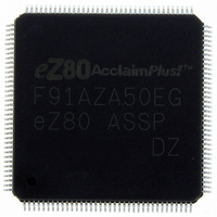
EZ80F91AZA50EG Zilog, EZ80F91AZA50EG Datasheet - Page 221

EZ80F91AZA50EG
Manufacturer Part Number
EZ80F91AZA50EG
Description
IC ACCLAIM MCU 256KB 144LQFP
Manufacturer
Zilog
Series
eZ80® AcclaimPlus!™r
Datasheet
1.EZ80F91AZA50SG.pdf
(387 pages)
Specifications of EZ80F91AZA50EG
Core Processor
Z8
Core Size
8-Bit
Speed
50MHz
Connectivity
Ethernet, I²C, IrDA, SPI, UART/USART
Peripherals
Brown-out Detect/Reset, POR, PWM, WDT
Number Of I /o
32
Program Memory Size
256KB (256K x 8)
Program Memory Type
FLASH
Ram Size
16K x 8
Voltage - Supply (vcc/vdd)
3 V ~ 3.6 V
Oscillator Type
Internal
Operating Temperature
-40°C ~ 105°C
Package / Case
144-LQFP
Processor Series
EZ80F91x
Core
eZ80
Data Bus Width
8 bit
Data Ram Size
16 KB
Interface Type
I2C, IrDA, SPI
Maximum Clock Frequency
50 MHz
Number Of Programmable I/os
32
Number Of Timers
4
Operating Supply Voltage
3 V to 3.6 V
Maximum Operating Temperature
+ 105 C
Mounting Style
SMD/SMT
Development Tools By Supplier
eZ80F910300ZCOG
Minimum Operating Temperature
- 40 C
For Use With
269-4712 - KIT DEV ENCORE 32 SERIES269-4671 - BOARD ZDOTS SBC Z80ACCLAIM PLUS269-4561 - KIT DEV FOR EZ80F91 W/C-COMPILER269-4560 - KIT DEV FOR EZ80F91 W/C-COMPILER
Lead Free Status / RoHS Status
Lead free / RoHS Compliant
Eeprom Size
-
Data Converters
-
Lead Free Status / Rohs Status
Details
Other names
269-4563
Available stocks
Company
Part Number
Manufacturer
Quantity
Price
- Current page: 221 of 387
- Download datasheet (5Mb)
I
PS027001-0707
2
C Serial I/O Interface
I
2
C General Characteristics
The Inter-Integrated Circuit (I
that operates in four modes:
•
•
•
•
The I
SDA are bidirectional lines connected to a positive supply voltage via an external pull-up
resistor. When the bus is free, both lines are High. The output stages of devices connected
to the bus must be configured as open-drain outputs. Data on the I
a rate of up to 100 kbps in STANDARD mode, or up to 400 kbps in FAST mode. One
clock pulse is generated for each data bit transferred.
Clocking Overview
If another device on the I
the I
determined by the device that generates the shortest High clock period. The Low period of
the clock is determined by the device that generates the longest Low clock period.
The Low period of the clock is stretched by a slave to slow down the bus master. The Low
period is also stretched for handshaking purposes. This result is accomplished after each
bit transfer or each byte transfer. The I
the IFLG bit in the I2C_CTL register is cleared to 0.
Bus Arbitration Overview
In MASTER mode, the I
a logic 1. If another device on the bus overrules and pulls the SDA signal Low, arbitration
is lost. If arbitration is lost during the transmission of a data byte or a Not Acknowledge
(NACK) bit, the I
an address, the I
the general call address.
MASTER TRANSMIT
MASTER RECEIVE
SLAVE TRANSMIT
SLAVE RECEIVE
2
2
C synchronizes its clock to the I
C interface consists of a Serial Clock (SCL) and Serial Data (SDA). Both SCL and
2
C switches to SLAVE mode so that it recognizes its own slave address or
2
C returns to an idle state. If arbitration is lost during the transmission of
2
2
C checks that each transmitted logic 1 appears on the I
C bus drives the clock line when the I
2
C) serial I/O bus is a two-wire communication interface
2
2
C bus clock. The High period of the clock is
C stretches the clock after each byte transfer until
2
Product Specification
C is in MASTER mode,
2
C bus are transferred at
I
2
C Serial I/O Interface
eZ80F91 ASSP
2
C bus as
213
Related parts for EZ80F91AZA50EG
Image
Part Number
Description
Manufacturer
Datasheet
Request
R

Part Number:
Description:
Communication Controllers, ZILOG INTELLIGENT PERIPHERAL CONTROLLER (ZIP)
Manufacturer:
Zilog, Inc.
Datasheet:

Part Number:
Description:
KIT DEV FOR Z8 ENCORE 16K TO 64K
Manufacturer:
Zilog
Datasheet:

Part Number:
Description:
KIT DEV Z8 ENCORE XP 28-PIN
Manufacturer:
Zilog
Datasheet:

Part Number:
Description:
DEV KIT FOR Z8 ENCORE 8K/4K
Manufacturer:
Zilog
Datasheet:

Part Number:
Description:
KIT DEV Z8 ENCORE XP 28-PIN
Manufacturer:
Zilog
Datasheet:

Part Number:
Description:
DEV KIT FOR Z8 ENCORE 4K TO 8K
Manufacturer:
Zilog
Datasheet:

Part Number:
Description:
CMOS Z8 microcontroller. ROM 16 Kbytes, RAM 256 bytes, speed 16 MHz, 32 lines I/O, 3.0V to 5.5V
Manufacturer:
Zilog, Inc.
Datasheet:

Part Number:
Description:
Low-cost microcontroller. 512 bytes ROM, 61 bytes RAM, 8 MHz
Manufacturer:
Zilog, Inc.
Datasheet:

Part Number:
Description:
Z8 4K OTP Microcontroller
Manufacturer:
Zilog, Inc.
Datasheet:

Part Number:
Description:
CMOS SUPER8 ROMLESS MCU
Manufacturer:
Zilog, Inc.
Datasheet:

Part Number:
Description:
SL1866 CMOSZ8 OTP Microcontroller
Manufacturer:
Zilog, Inc.
Datasheet:

Part Number:
Description:
SL1866 CMOSZ8 OTP Microcontroller
Manufacturer:
Zilog, Inc.
Datasheet:

Part Number:
Description:
OTP (KB) = 1, RAM = 125, Speed = 12, I/O = 14, 8-bit Timers = 2, Comm Interfaces Other Features = Por, LV Protect, Voltage = 4.5-5.5V
Manufacturer:
Zilog, Inc.
Datasheet:

Part Number:
Description:
Manufacturer:
Zilog, Inc.
Datasheet:


