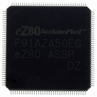
EZ80F91AZA50EG Zilog, EZ80F91AZA50EG Datasheet - Page 380

EZ80F91AZA50EG
Manufacturer Part Number
EZ80F91AZA50EG
Description
IC ACCLAIM MCU 256KB 144LQFP
Manufacturer
Zilog
Series
eZ80® AcclaimPlus!™r
Datasheet
1.EZ80F91AZA50SG.pdf
(387 pages)
Specifications of EZ80F91AZA50EG
Core Processor
Z8
Core Size
8-Bit
Speed
50MHz
Connectivity
Ethernet, I²C, IrDA, SPI, UART/USART
Peripherals
Brown-out Detect/Reset, POR, PWM, WDT
Number Of I /o
32
Program Memory Size
256KB (256K x 8)
Program Memory Type
FLASH
Ram Size
16K x 8
Voltage - Supply (vcc/vdd)
3 V ~ 3.6 V
Oscillator Type
Internal
Operating Temperature
-40°C ~ 105°C
Package / Case
144-LQFP
Processor Series
EZ80F91x
Core
eZ80
Data Bus Width
8 bit
Data Ram Size
16 KB
Interface Type
I2C, IrDA, SPI
Maximum Clock Frequency
50 MHz
Number Of Programmable I/os
32
Number Of Timers
4
Operating Supply Voltage
3 V to 3.6 V
Maximum Operating Temperature
+ 105 C
Mounting Style
SMD/SMT
Development Tools By Supplier
eZ80F910300ZCOG
Minimum Operating Temperature
- 40 C
For Use With
269-4712 - KIT DEV ENCORE 32 SERIES269-4671 - BOARD ZDOTS SBC Z80ACCLAIM PLUS269-4561 - KIT DEV FOR EZ80F91 W/C-COMPILER269-4560 - KIT DEV FOR EZ80F91 W/C-COMPILER
Lead Free Status / RoHS Status
Lead free / RoHS Compliant
Eeprom Size
-
Data Converters
-
Lead Free Status / Rohs Status
Details
Other names
269-4563
Available stocks
Company
Part Number
Manufacturer
Quantity
Price
- Current page: 380 of 387
- Download datasheet (5Mb)
open-source mode 51
Open-source output 50
open-source output 11, 12, 13, 14, 15, 16, 17, 18,
19
Operating Modes, I2C 218
Operation of the eZ80F91 Device during ZDI Break
Points 242
Ordering Information 362
Output Compare 128
Output compare mode 143
output compare mode 127, 128, 130, 133
overrun condition, receiver 178
Overrun error 193
overrun error 175, 177, 185
Overview, Phase-Locked Loop 269
P
PA7 150
Packaging 361
Page Erase 101
page erase 112
Page Erase operation 113
page erase operation 101, 109
PAIR_EN 153, 154
parity error 177, 188, 193
Part Number Description 363
PB0 17
PB1 17
PB2 17
PB3 18
PB4 18
PB5 18
PB6 19
PB7 19
PC0 14, 20
PC1 14, 20
PC2 15, 20
PC3 15, 21
PC4 15, 21
PC5 16, 21
PC6 16, 22
PC7 16, 22
PD0 11, 200
PS027001-0707
PD1 11, 200
PD2 12, 200
PD3 12
PD4 12
PD5 13
PD6 13
PD7 13, 200
Phase Frequency Detector 269
Phase Frequency Detector, PLL 270
PHI 19, 265
PHI Clock output 48
PHY 22, 24, 28, 29, 296, 300, 318, 319, 329,
330, 331
PHY, MII 292, 317
Pin Characteristics 6
Pin Coverage, JTAG Boundary Scan 263
Pin Description 4
PLL Characteristics 276
PLL Control Register 0 273
PLL Control Register 1 274
PLL Divider Control Register—Low and High
Bytes 272
PLL Loop Filter 13
PLL Normal Operation 271
PLL Registers 272
PLL_VDD 272
PLL_VSS 272
Poll Mode Transfers 181
POP, Op Code Map 284, 286, 288
POR Voltage Threshold 345
POR voltage threshold 42
POR/VBO analog RESET duration 345
POR/VBO DC current consumption 345
POR/VBO Hysteresis 345
Port A 20, 21, 47, 49, 58, 62, 63, 145
Port x Alternate Register 1 56
Port x Alternate Register 2 56
Port x Data Direction Registers 55
Port x Data Registers 55
Potential Hazards of Enabling Bus Requests During
Debug Mode 243
Power connections 2
Power Requirement to the Phase-Locked Loop
Function 272
Product Specification
eZ80F91 ASSP
372
Related parts for EZ80F91AZA50EG
Image
Part Number
Description
Manufacturer
Datasheet
Request
R

Part Number:
Description:
Communication Controllers, ZILOG INTELLIGENT PERIPHERAL CONTROLLER (ZIP)
Manufacturer:
Zilog, Inc.
Datasheet:

Part Number:
Description:
KIT DEV FOR Z8 ENCORE 16K TO 64K
Manufacturer:
Zilog
Datasheet:

Part Number:
Description:
KIT DEV Z8 ENCORE XP 28-PIN
Manufacturer:
Zilog
Datasheet:

Part Number:
Description:
DEV KIT FOR Z8 ENCORE 8K/4K
Manufacturer:
Zilog
Datasheet:

Part Number:
Description:
KIT DEV Z8 ENCORE XP 28-PIN
Manufacturer:
Zilog
Datasheet:

Part Number:
Description:
DEV KIT FOR Z8 ENCORE 4K TO 8K
Manufacturer:
Zilog
Datasheet:

Part Number:
Description:
CMOS Z8 microcontroller. ROM 16 Kbytes, RAM 256 bytes, speed 16 MHz, 32 lines I/O, 3.0V to 5.5V
Manufacturer:
Zilog, Inc.
Datasheet:

Part Number:
Description:
Low-cost microcontroller. 512 bytes ROM, 61 bytes RAM, 8 MHz
Manufacturer:
Zilog, Inc.
Datasheet:

Part Number:
Description:
Z8 4K OTP Microcontroller
Manufacturer:
Zilog, Inc.
Datasheet:

Part Number:
Description:
CMOS SUPER8 ROMLESS MCU
Manufacturer:
Zilog, Inc.
Datasheet:

Part Number:
Description:
SL1866 CMOSZ8 OTP Microcontroller
Manufacturer:
Zilog, Inc.
Datasheet:

Part Number:
Description:
SL1866 CMOSZ8 OTP Microcontroller
Manufacturer:
Zilog, Inc.
Datasheet:

Part Number:
Description:
OTP (KB) = 1, RAM = 125, Speed = 12, I/O = 14, 8-bit Timers = 2, Comm Interfaces Other Features = Por, LV Protect, Voltage = 4.5-5.5V
Manufacturer:
Zilog, Inc.
Datasheet:

Part Number:
Description:
Manufacturer:
Zilog, Inc.
Datasheet:


